Nanofiber surfaces for use in enhanced surface area applications

Active Publication Date: 2006-07-20
NANOSYS INC
View PDF59 Cites 304 Cited by
  • Summary
  • Abstract
  • Description
  • Claims
  • Application Information

AI Technical Summary

Benefits of technology

[0021] The invention also includes separation systems/devices having a separation substrate comprising a plurality of nanofibers attached thereto, wherein the substrate comprises an enhanced surface area, which area is from about 2× to about 10,000× or more greater in area than a planar substrate of substantially similar footprint dimensions; one or more source of one or more material to be separated; and, a fluid delivery device. Some embodiments of such systems/devices include wherein members of the plurality of nanofibers comprise an average length of from about 1 micron to at least about 200 microns or more; an average diameter of from about 5 nm to at least about 1 micron or more, and an aver

Problems solved by technology

In almost all instances, however, the efficiency or use of such processes and devices is limited, at least in part, by the area of the surface which is in contact with the one or more compound or desired constituent (e.g., the liquid, gas, etc.).
First, space limitations are of concern.
Thus, the action to be accomplished can be limited by the number of functional units, which is in turn limited by the unit area or footprint of the surface which contains the functional units.
However, besides being inelegant, such response is often problematic due to cost restraints and size limitations imposed on the footprint itself (e.g., the reaction might need to be performed in a limited space in a device, etc.)
Second, such processes and devices are often also limited in terms of resolution or sensitivity.
For example, in situations such as detection, the activity allowing detection of a compound or constituent can sometimes be ‘weak’ or difficult to detect.
In such situations, even increasing the footprint size might not be enough to improve detection, since a weak response is stil

Method used


Image

  • Nanofiber surfaces for use in enhanced surface area applications
  • Nanofiber surfaces for use in enhanced surface area applications
  • Nanofiber surfaces for use in enhanced surface area applications

Examples


example 1

i) EXAMPLE 1

Wicking on Nanofiber and Planar Substrates

[0309] To illustrate comparative wicking of liquids (here water) between a planar silicon surface and a nanofiber enhanced area substrate of the invention, a 1 uL drop of water was placed upon each. FIG. 28A, displays a graph comparing the wicking of the water, (measured in FIG. 28 as comparative evaporation) between the planar silicon surface and the nanofiber enhanced surface area substrate of the invention. As can be seen, wicking (and hence, in FIG. 28, evaporation as displayed by “% water loss”) occurs much more rapidly with the substrates of the invention. FIG. 28B displays the data for the graph in FIG. 28A.

example 2

ii) EXAMPLE 2

Exemplary Flow Assays of Nanofiber Substrates

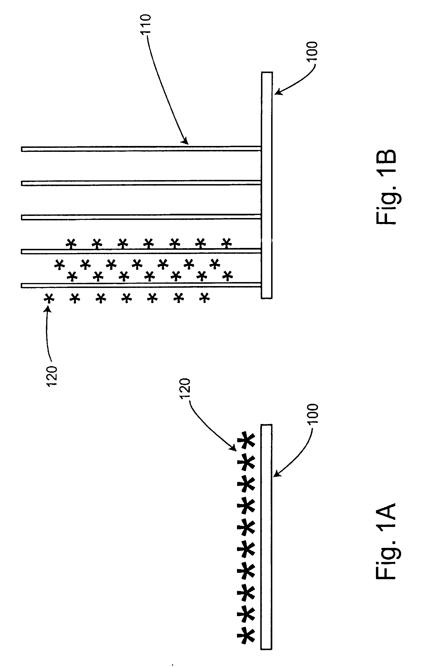
[0310]FIG. 29 shows a schematic of a nanofiber enhanced slide configured into a flow assay scheme. In FIG. 29, biotinylated BSA (i.e., a probe), 2900, was adsorbed at known positions along nanofiber tracks (in this instance nanowire tracks), 2910, on slide 2940. The tracks were generated by scraping the edge of a glass slide through a nanofiber field on a substrate. A solution containing fluorescently labeled streptavidin (i.e., a target) was applied to the tops of the tracks. 15 ul of SAv-647 in PBS / 0.1% BSA was followed by a total of 300 ul PBS / 0.1% BSA. The liquid, thus, wicked into the nanofiber tracks until it filled the interstitial space between the nanofibers. To continue the liquid flow and to wash through any unbound label, additional liquid was added at the top of the tracks and a filter paper wick, 2920, was placed at the bottom end of the tracks. The paper acted as a reservoir for the liquid that had traversed t...

example 3

iii) EXAMPLE 3

Exemplary Nanofiber Array Patterning

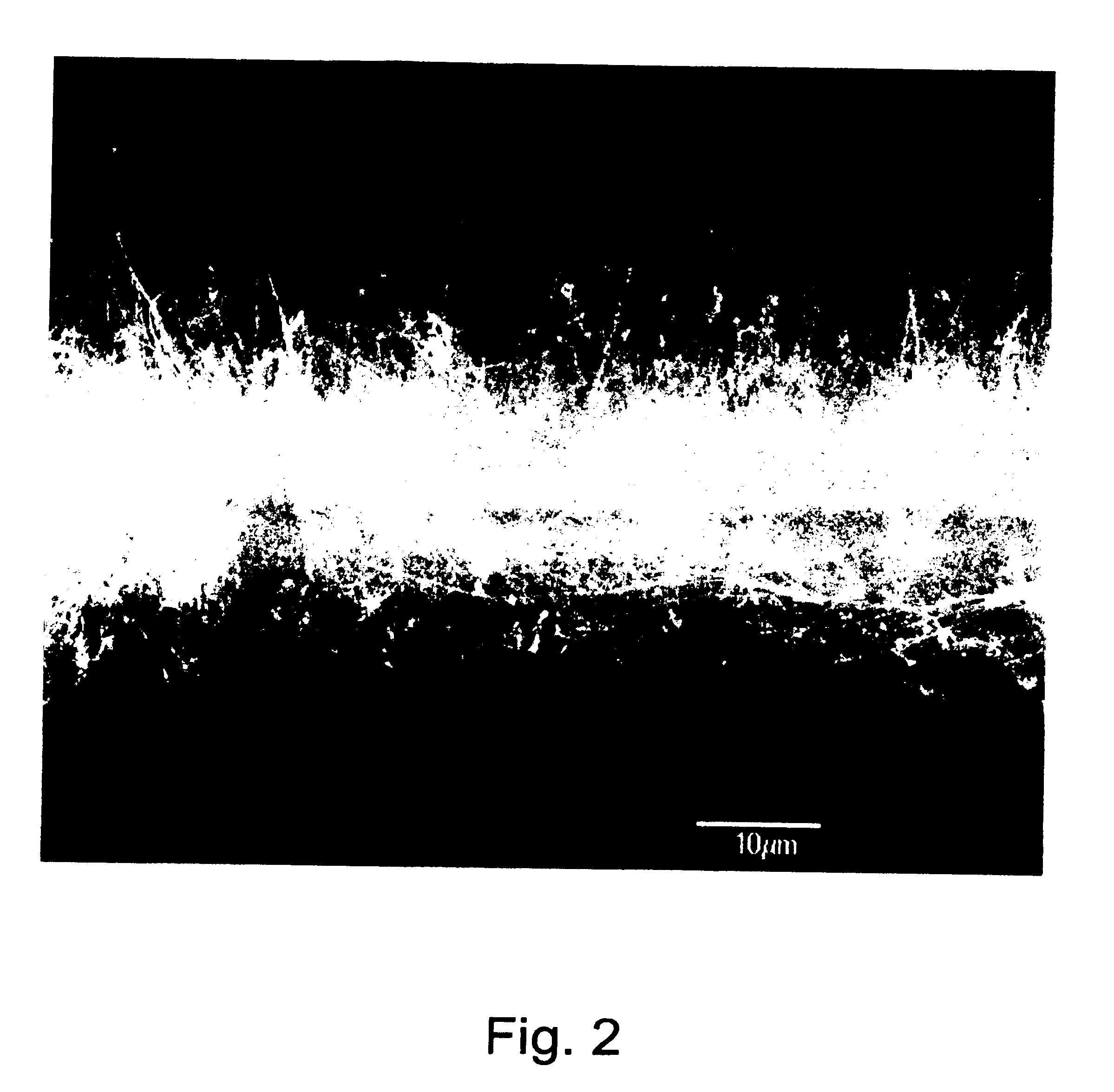
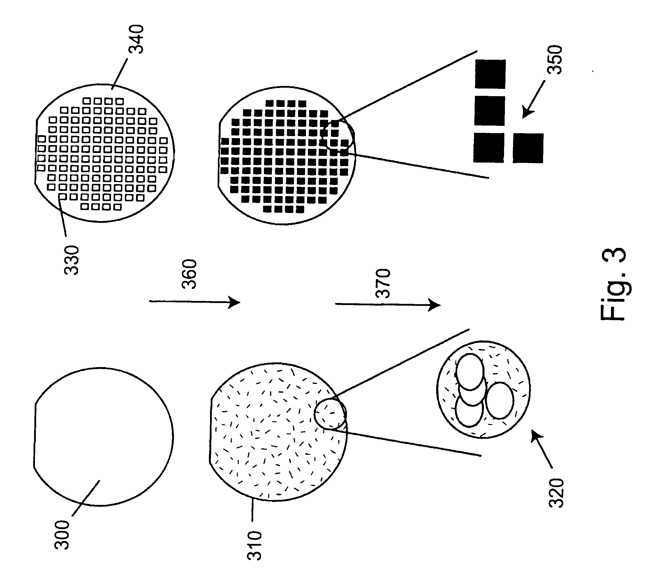
[0313] The ability to grow nanometer scale wires of defined diameter and length on various surfaces is illustrated in FIG. 7. FIG. 7 shows an example of an “extreme” surface with very high surface to volume ratios and yet without the complex etched architecture of other more traditional strategies for increasing surface area to volume (e.g. etched silicon). FIG. 7 shows SEM views of top and side views of a typical nanofiber surface, both patterned and unpatterned. The silicon nanofibers were grown out from a silicon wafer and the surfaces were therefore compatible with standard glass modification chemistries, etc. Although discussion herein primarily focuses on silicon wafers as the substrate for nanowire growth, as explained further above, the process can potentially be conducted on a wide variety of substrates that can have planar or complex geometries.

[0314] Examples of nanofiber arrays produced by masking process can be seen in...


PUM

PropertyMeasurementUnit
Lengthaaaaaaaaaa
Lengthaaaaaaaaaa
Lengthaaaaaaaaaa

Abstract

This invention provides novel nanofiber enhanced surface area substrates and structures comprising such substrates, as well as methods and uses for such substrates.

Description

CROSS-REFERENCE TO RELATED APPLICATIONS [0001] This application is a continuation-in-part of, and claims benefit of and priority to, U.S. Ser. No. 10 / 792,402, filed Mar. 2, 2004, and U.S. Provisional Application Nos. 60 / 468,606 filed May 5, 2003, and 60 / 468,390 filed May 6, 2003, all entitled “NANOFIBER SURFACES FOR USE IN ENHANCE SURFACE AREA APPLICATIONS.” These prior applications are hereby incorporated by reference in their entirety for all purposes.FIELD OF THE INVENTION [0002] The invention relates primarily to the field of nanotechnology. More specifically, the invention pertains to nanofibers, and nanofiber structures having enhanced surface areas, as well as to the use of such nanofibers and nanofiber structures in various applications. BACKGROUND OF THE INVENTION [0003] Numerous scientific and commercial processes involve the interaction of one or more compounds (often in liquid form or present in a liquid carrier or the like) with one or more surface area. Such surfaces c...

Claims


Application Information

Patent Timeline
IPC IPC(8): B32B19/00D02G3/00B32B9/00
CPCA61L2400/12Y10T428/2913B01J20/28007B01J20/28057B01J20/281B01J20/32B01J20/3242B01L3/5027B01L2200/16B01L2300/0636B01L2300/0681B01L2300/069B01L2300/161B01L2400/0406B82Y30/00D04H1/42F28D15/046G01N30/92G01N33/54346G01N33/54393H01J49/0418F28F2245/04F28F2245/02Y10S977/773Y10S977/762Y10S977/904Y10S977/813Y10S977/764Y10T428/29Y10T428/292Y10T428/2929Y10T428/298Y10T428/2918Y10T428/2915A61M1/1698B01J20/3204B01J20/321B01J20/3212B01J20/3219B01J20/3234B01J20/3236B01J20/3246B01J20/3265B01J20/327B01J20/3272B01J20/3274B01J20/3289B01J20/3291
Inventor DUBROW, ROBERTDANIELS, ROBERTPARCE, J.MURPHY, MATTHEWHAMILTON, JIMSCHER, ERIKSTUMBO, DAVENIU, CHUNMINGROMANO, LINDAGOLDMAN, JAYSAHI, VIJENDRAWHITEFORD, JEFFERY
Owner NANOSYS INC
Why Eureka
Try Eureka