Non-volatile memory device supporting high-parallelism test at wafer level

a memory device and wafer level technology, applied in the field of memory, can solve the problems of not reaching the target oxide thickness, significant stress on the oxide layer of the memory cells, and inability to detect the number of cells of the memory device that can work properly

Inactive Publication Date: 2006-07-20
STMICROELECTRONICS SRL +1
View PDF10 Cites 11 Cited by
  • Summary
  • Abstract
  • Description
  • Claims
  • Application Information

AI Technical Summary

Benefits of technology

[0027] This implementation is very simple.

Problems solved by technology

However, due to technology reasons, there is a not negligible number of cells of the memory device that can work properly for a certain number of cycles before failing.
The basic physical phenomenon occurring is that any read, program and erase operation internally generates very high voltages that cause a significant stress on oxide layers of the memory cells.
Indeed, the thickness of the oxide layers is chosen in order to guarantee product reliability; however, due to many different production problems, it is possible that target oxide thickness is not reached.
This phenomenon is getting more and more evident and dangerous with the technology scaling.
In order to detect the memory devices with thinner oxide layers (also called “early failing devices”), it is not possible to apply voltages higher than the ones usually needed for standard operations.
In fact, such high voltages might damage good oxide layers as well; moreover, their generation would involve a significant waste of area of a silicon chip wherein the memory device is integrated.
In any case, the time required to perform the test process is very long.
This drawback is particular acute in modern memory devices with high density; for example, it is possible to have memory devices of the NAND flash type with a capacity up to 4 Gbit.
However, the charge pump circuits that generate the high voltages necessary to execute the program operation have to be over-dimensioned, in such a way to support the higher load due to the parallel operations.
This cases an excessive waste of area on the chip.
The main drawback of this solution is that each memory device normally has a number of pads equal to 15-16, so that a probe-card with a very high number of probes is required.
However, this strongly increases the cost of the probe-card.
However, the test process time is not significantly reduced.
Moreover, in this case it is not possible to recreate the conditions that can cause the early failing of the memory devices exactly.
A drawback of this solution is that it requires additional integrated structures (wasting area on the chip).
In any case, a common problem in the test process sphere is that a user may activate (accidentally or not) the test process when the memory device is in operation.

Method used


Image

  • Non-volatile memory device supporting high-parallelism test at wafer level
  • Non-volatile memory device supporting high-parallelism test at wafer level
  • Non-volatile memory device supporting high-parallelism test at wafer level

Examples


Embodiment Construction

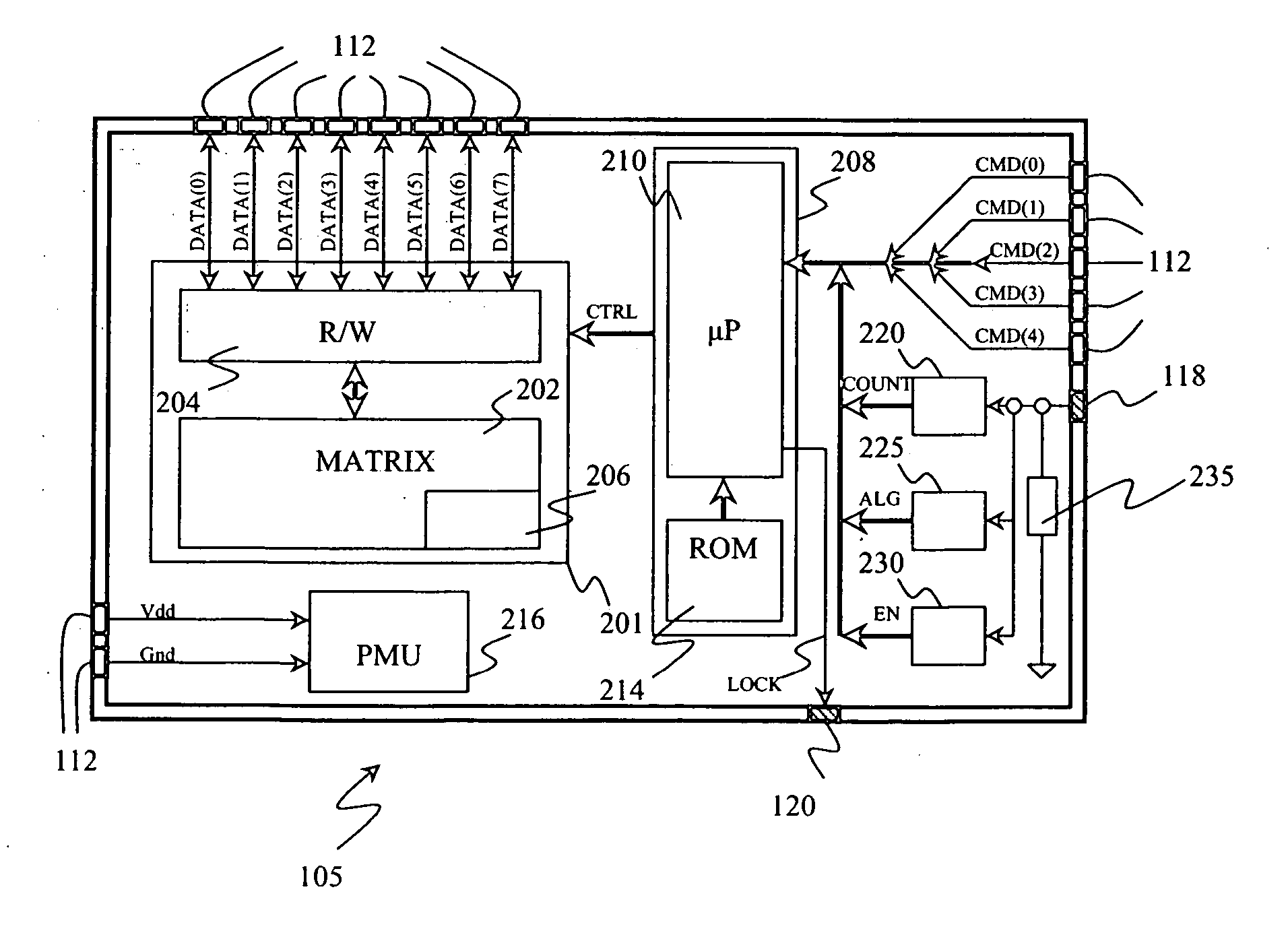
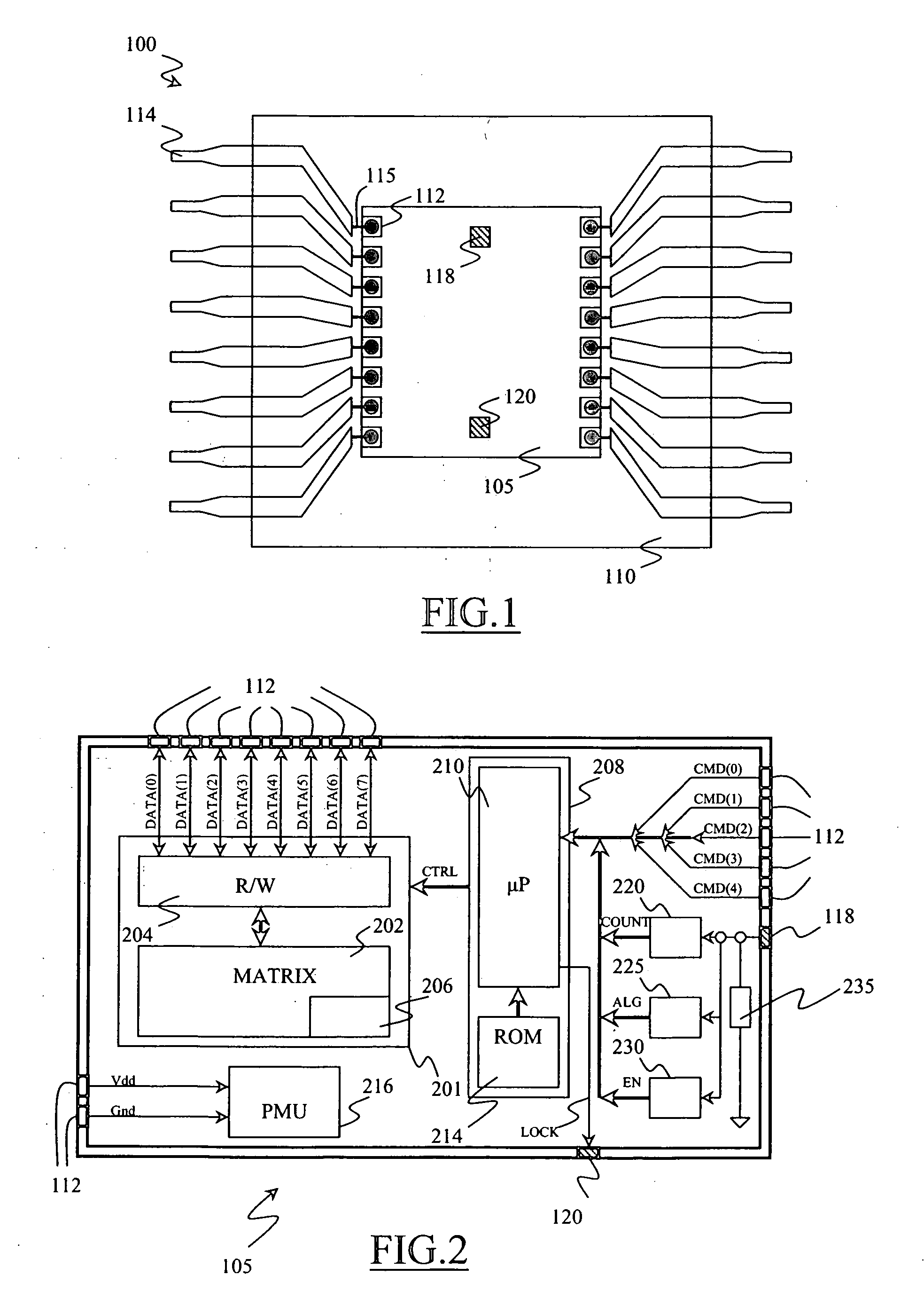
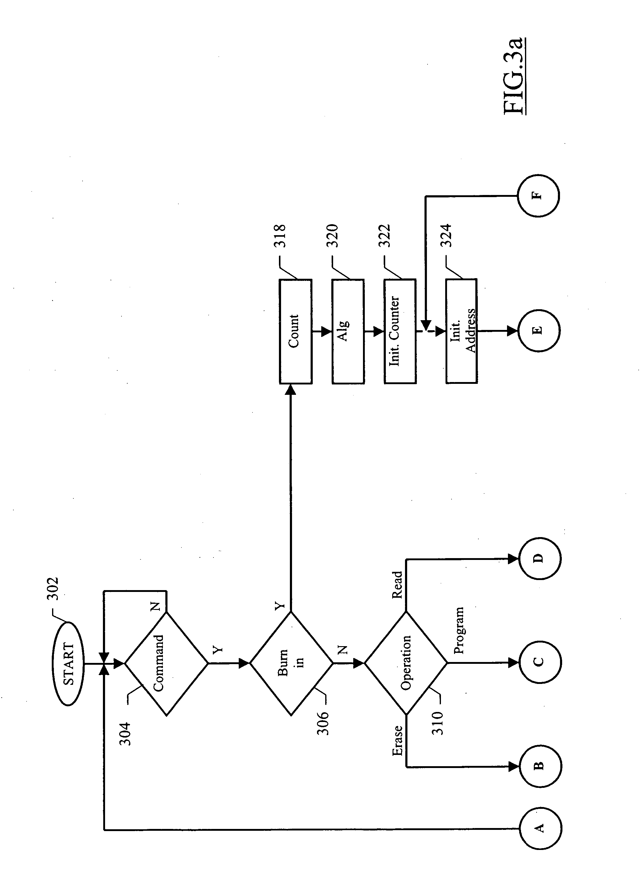
[0042] In the following description, numerous specific details are given to provide a thorough understanding of embodiments of the invention. One skilled in the relevant art will recognize, however, that the invention can be practiced without one or more of the specific details, or with other methods, components, materials, etc. In other instances, well-known structures, materials, or operations are not shown or described in detail to avoid obscuring aspects of the invention.

[0043] Reference throughout this specification to “one embodiment” or “an embodiment” means that a particular feature, structure, or characteristic described in connection with the embodiment is included in at least one embodiment of the present invention. Thus, the appearances of the phrases “in one embodiment” or “in an embodiment” in various places throughout this specification are not necessarily all referring to the same embodiment. Furthermore, the particular features, structures, or characteristics may b...


PUM


Abstract

A non-volatile memory device includes a chip of semiconductor material. The chip includes a memory and control means for performing a programming operation, an erasing operation and a reading operation on the memory in response to corresponding external commands. The chip further includes testing means for performing at least one test process including the repetition of at least one of said operations by the control means, and a single access element for enabling the testing means.

Description

TECHNICAL FIELD [0001] The present disclosure generally relates to the memory field. More specifically but not exclusively, the present disclosure relates to the testing of semiconductor memory devices. BACKGROUND INFORMATION [0002] The test of semiconductor devices, and particularly of non-volatile memory devices is a very critical activity. The object of any test process is of verifying that each device under analysis operates correctly according to its specifications. This is of the utmost importance for ensuring a high level of quality of the corresponding production process. [0003] A typical example is that of memory devices of the flash type with a NAND architecture, which must guarantee a very high reliability (such as 100K operation cycles and 10 years of data retention). However, due to technology reasons, there is a not negligible number of cells of the memory device that can work properly for a certain number of cycles before failing. The basic physical phenomenon occurri...

Claims


Application Information

Patent Timeline
Patent Type & Authority Applications(United States)
IPC IPC(8): G11C29/00
CPCG11C16/04G11C29/006G11C29/1201G11C29/16G11C29/46G11C2029/2602
Inventor LOMAZZI, GUIDORENNA, ILARIAMACCARONE, MARCO
Owner STMICROELECTRONICS SRL
Why Eureka
Try Eureka