Method and composition for electro-chemical-mechanical polishing

a technology of electrochemical and mechanical polishing, applied in the direction of electrolysis components, manufacturing tools, aqueous dispersions, etc., can solve the problems of large processing difficulty, inability to efficiently planarize sub-micron height differences, and inability to achieve efficient planarization process

Inactive Publication Date: 2006-07-27
IBM CORP
View PDF24 Cites 41 Cited by
  • Summary
  • Abstract
  • Description
  • Claims
  • Application Information

AI Technical Summary

Benefits of technology

[0005] The present invention provides compositions for electro-chemical-mechanical polishing (e-CMP) of chip interconnect materials. These compositions comprise a first component, heretofore “solvent”, either water or a mixture of water and one or more organic solvents such as propylene glycol, glycerol or ethanol; and a second component, heretofore “electrolyte”, selected from the group consisting of: mineral acids and organic acids comprising phosphonic, sulfonic and carboxylic acids, such as phosphoric acid, sulfuric acid, 1-hydroxyethane-1,1-diphosphonic acid (HEDP), phytic acid, 3-(4-morpholino)propanesulfonic acid (MOPS) and acetic acid, and mixtures of aforesaid acids and their salts, including acid salts, with sodium, potassium, ammonium, and protonated amine or azole ions such as ethanaminium, ethanolaminium and N-methylimidazolium These compositions further comprise at least one additional component, heretofore “inhibitor”, selected from the group consisting of: an anionic surfactant such as long chain alkylsulfonates having from 4 to 16 carbon atoms, a non-ionic surfactant such as poly(ethylene glycol), a cationic surfactant such as long chain alkyltrimethylammonium hydrogensulfate with 4 to 18 carbon atoms in the alkyl chain, and a surface active organic compound containing nitrogen or sulfur such as: an N-alkylimidazole with an alkyl group having from 1 to 8 carbon atoms, benzotriazole (BTA), derivatives of BTA, 3-mercaptopropanoic acid, 2-mercapto-1-methylimidazole. Optionally these compositions can also contain a soluble salt of the metal being removed, for example copper sulfate when the metal being removed is copper.
[0006] The present invention further provides methods for electrochemical-mechanical polishing (e-CMP) of chip interconnect materials using the above compositions. In addition, the present invention provides methods involving the use of a pad that that allows the passage of current between a cathode and the chip interconnect material being polished. Such a pad may, for example, be selected from the group consisting of: a porous pad, an electroactive pad, a perforated pad, a fixed abrasive pad, and at least one pad having a surface area that is smaller than the cathode.

Problems solved by technology

Such processing represents a significant technical challenge, in large part due to the small thickness of copper available for consumption during the planarization process.
However, routine electropolishing of a highly conductive surface such as copper does not typically lead to efficient planarization of sub-micron height differences; rather, the electrodissolution of metal tends to be conformal.
In this regard, the potential differences and the differences in concentration gradients at different points along the surface are generally too small to enable an efficient planarization process.
However, the downward and shear force that CMP applies on the wafer surface can be damaging to the new generations of low-k dielectrics, which tend to be quite fragile.
In order to compensate, CMP can be used with a much lower downward and shear force, but these forces generally result in a considerable reduction of the polishing rate.
Given that CMP processes can be expected to be relatively costly in terms of factory floor space and consumables, lower polishing rates are generally considered undesirable.

Method used


Image

  • Method and composition for electro-chemical-mechanical polishing
  • Method and composition for electro-chemical-mechanical polishing
  • Method and composition for electro-chemical-mechanical polishing

Examples


Embodiment Construction

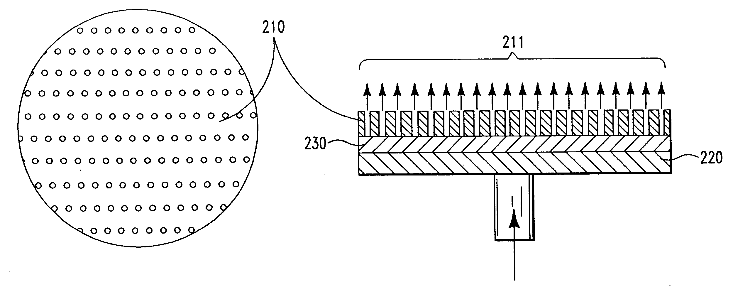
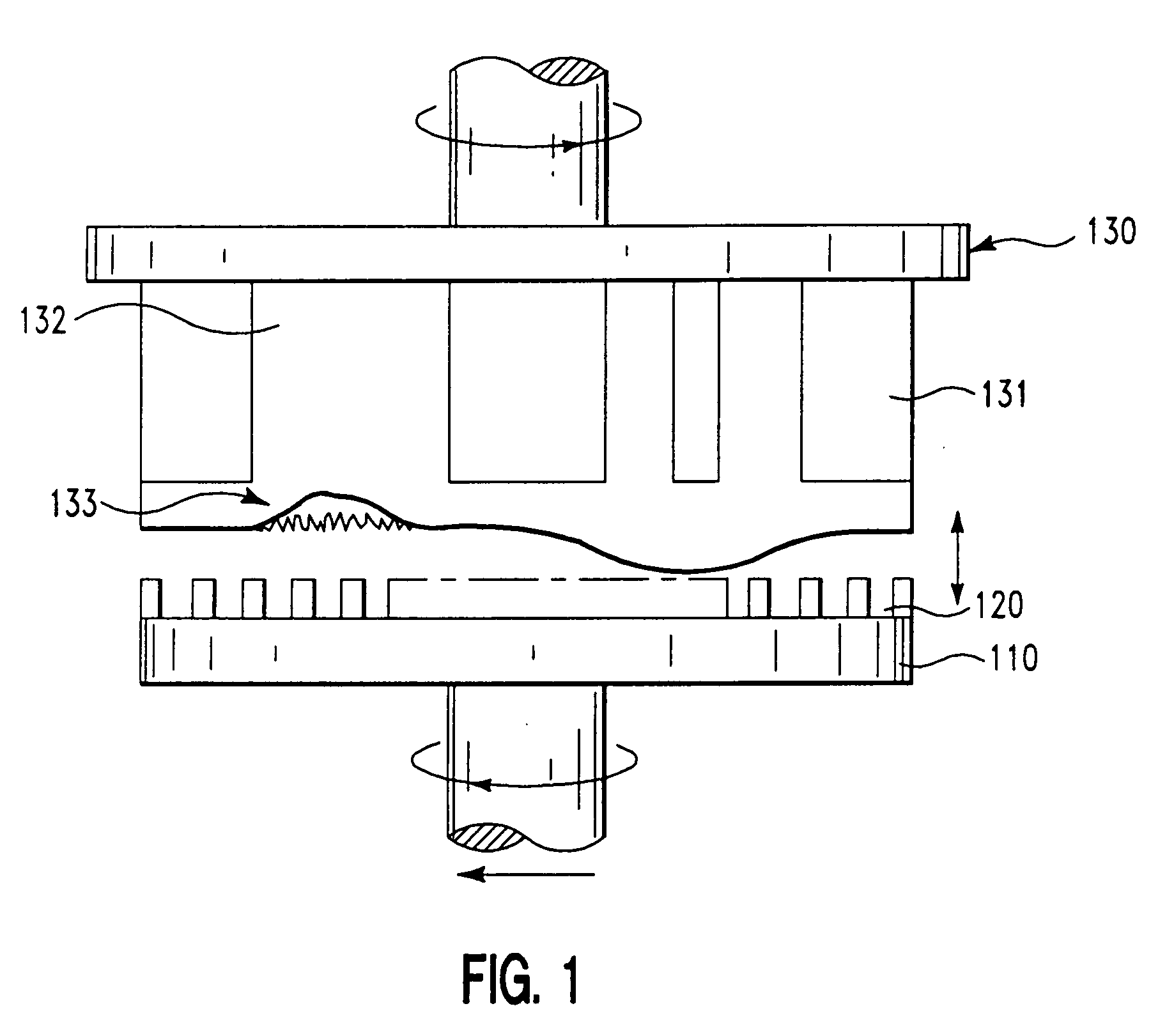
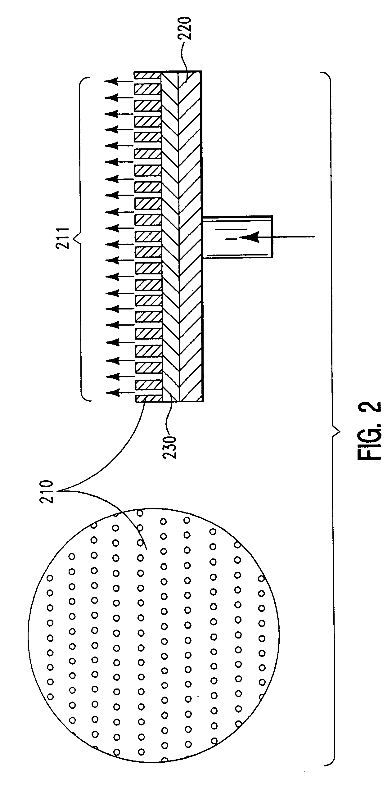
[0024] The present invention relates to methods and compositions for achieving planarization of silicon chip interconnects, such as copper interconnects. Specifically, the present invention relates to methods and compositions for electro-chemical-mechanical polishing (e-CMP) of such interconnects, in which a wafer serves as an anode in an electrical circuit and the effect of the current is coupled with the mechanical action of a pad. The action of the pad can involve actual contact and pressure, creation of viscous shear at close proximity to a substrate, or a combination of both.

[0025] Electro-chemical-mechanical polishing allows for more prominent points on a surface (“mounds”) to be affected more than lower spots. This effect is achieved via the formation of an inhibiting layer or film on a surface, in which the film is disturbed in greater proportion over the mounds, which, as a result, are polished away faster than the rest of the surface. Conversely, recessed areas are polish...


PUM

PropertyMeasurementUnit
thicknessaaaaaaaaaa
thicknessaaaaaaaaaa
pHaaaaaaaaaa

Abstract

Methods and compositions for electro-chemical-mechanical polishing (e-CMP) of silicon chip interconnect materials, such as copper, are provided. The methods include the use of compositions according to the invention in combination with pads having various configurations.

Description

FIELD OF THE INVENTION [0001] The present invention relates to methods and chemical compositions that can be used for electrochemical-mechanical polishing (e-CMP) of a silicon chip interconnect material, such as copper. Specifically, the present invention relates to e-CMP methods and compositions that can be used to achieve improved planarization of silicon chip interconnect materials. BACKGROUND OF THE INVENTION [0002] The electrodeposition of copper for silicon chip interconnects is considered to be an important part of the modem microelectronics process. Such interconnects are often provided by depositing copper onto a seed layer, which covers a conductive liner, into lithographically generated lines and vias, and an excess of copper—often called “overburden”—is deposited on top of these features and across the field, usually to a thickness of about 0.5 microns to about 1.5 microns. Typically, this overburden layer is not very planar. It often contains mounds on top of high aspec...

Claims


Application Information

Patent Timeline
Patent Type & Authority Applications(United States)
IPC IPC(8): B23H3/00
CPCB23H5/08C09G1/04C25F3/02H01L21/32125
Inventor ANDRICACOS, PANAYOTIS C.CANAPERI, DONALD F.COOPER, EMANUEL I.COTTE, JOHN M.DELIGIANNI, HARIKLIAECONOMIKOS, LAERTISEDELSTEIN, DANIEL C.FRANZ, SILVIAPRANATHARTHIHARAN, BALASUBRAMANIANKRISHNAN, MAHADEVAIYERMANSSON, ANDREW P.WALTON, ERICK G.WEST, ALAN C.ANDRICACOS, CALIOPI
Owner IBM CORP
Why Eureka
Try Eureka