Structure for CMOS image sensor

a technology of image sensor and structure, applied in the field of semiconductor devices, can solve the problems of reducing the maximum output signal, increasing the output signal, and high susceptibility to nois

Active Publication Date: 2006-07-27
TAIWAN SEMICON MFG CO LTD
View PDF24 Cites 29 Cited by
  • Summary
  • Abstract
  • Description
  • Claims
  • Application Information

AI Technical Summary

Benefits of technology

[0004] Typically, CMOS image sensors are fabricated utilizing a capacitance within the photo-diode and a floating capacitance created between transistor connections. These capacitances, however, are characterized by small capacitance values, which cause a high susceptibility to noise and reduce the maximum output signal. Attempts have been made to increase the signal generated by a photo-diode, but these typically only increase the electrical charge generated by the photo-diode and do not necessarily increase the output signal.

Problems solved by technology

These capacitances, however, are characterized by small capacitance values, which cause a high susceptibility to noise and reduce the maximum output signal.
Attempts have been made to increase the signal generated by a photo-diode, but these typically only increase the electrical charge generated by the photo-diode and do not necessarily increase the output signal.
This type of transistor, however, introduces a silicon surface trap and leakage.
As a result, noise on the output signal increases and the dark signal increases.

Method used


Image

  • Structure for CMOS image sensor
  • Structure for CMOS image sensor
  • Structure for CMOS image sensor

Examples


Embodiment Construction

[0020] The making and using of the presently preferred embodiments are discussed in detail below. It should be appreciated, however, that the present invention provides many applicable inventive concepts that can be embodied in a wide variety of specific contexts. The specific embodiments discussed are merely illustrative of specific ways to make and use the invention, and do not limit the scope of the invention.

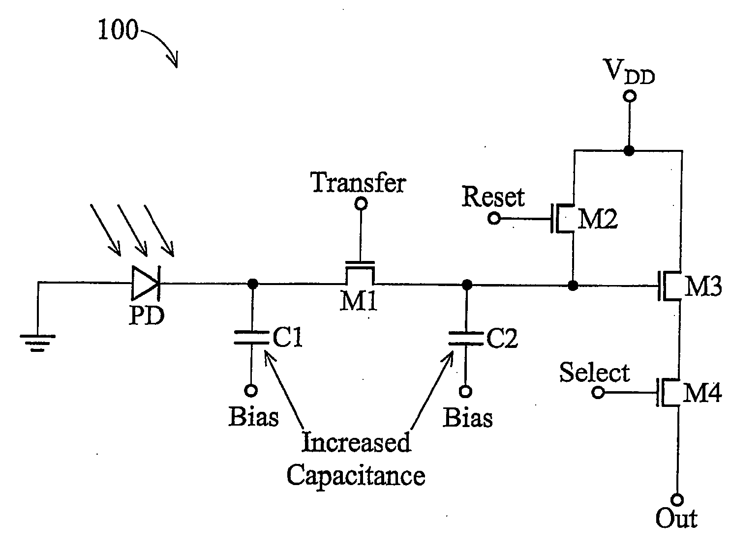
[0021] Referring first to FIG. 1, a schematic of a 4-transistor (4T) CMOS pixel 100 having increased capacitance in accordance with an embodiment of the present invention is shown. The 4T image pixel comprises a photo-diode PD having an anode coupled to ground and a cathode coupled to a first plate of a first capacitor C1 and a source connection of a first transistor M1. The second plate of the first capacitor C1 may be coupled to a bias, such as ground, VDD, 0.5*VDD, or the like. The first transistor M1 is a transfer transistor and has a gate electrode coupled to a transfe...


PUM


Abstract

A CMOS image sensor having increased capacitance that allows a photo-diode to generate a larger current is provided. The increased capacitance reduces noise and the dark signal. The image sensor utilizes a transistor having nitride spacers formed on a buffer oxide layer. Additional capacitance may be provided by various capacitor structures, such as a stacked capacitor, a planar capacitor, a trench capacitor, a MOS capacitor, a MIM / PIP capacitor, or the like. Embodiments of the present invention may be utilized in a 4-transistor pixel or a 3-transistor pixel configuration.

Description

TECHNICAL FIELD [0001] The present invention relates generally to semiconductor devices, and more particularly, to a complementary metal-oxide-semiconductor image sensor. BACKGROUND [0002] Complementary metal-oxide semiconductor (CMOS) image sensors are gaining in popularity over traditional charged-coupled devices (CCDs) due to certain advantages inherent in the CMOS image sensors. In particular, CMOS image sensors typically require lower voltages, consume less power, enable random access to image data, may be fabricated with compatible CMOS processes, and enable integrated single-chip cameras. [0003] Generally, CMOS image sensors utilize light-sensitive CMOS circuitry to convert light energy into electrical energy. The light-sensitive CMOS circuitry typically comprises a photo-diode formed in a silicon substrate. As the photo-diode is exposed to light, an electrical charge is induced in the photo-diode. The photo-diode is typically coupled to a MOS switching transistor, which is u...

Claims


Application Information

Patent Timeline
Patent Type & Authority Applications(United States)
IPC IPC(8): H04N5/335
CPCH01L27/14603H01L27/14609H01L27/14643H01L27/14689H04N5/3559H04N5/361H04N5/374H04N5/37452H04N25/59H04N25/63H04N25/771H04N25/76
Inventor YAUNG, DUN-NIANHUANG, KUO-CHINGCHIEN, HO-CHINGWUU, SHOU-GWO
Owner TAIWAN SEMICON MFG CO LTD
Why Eureka
Try Eureka