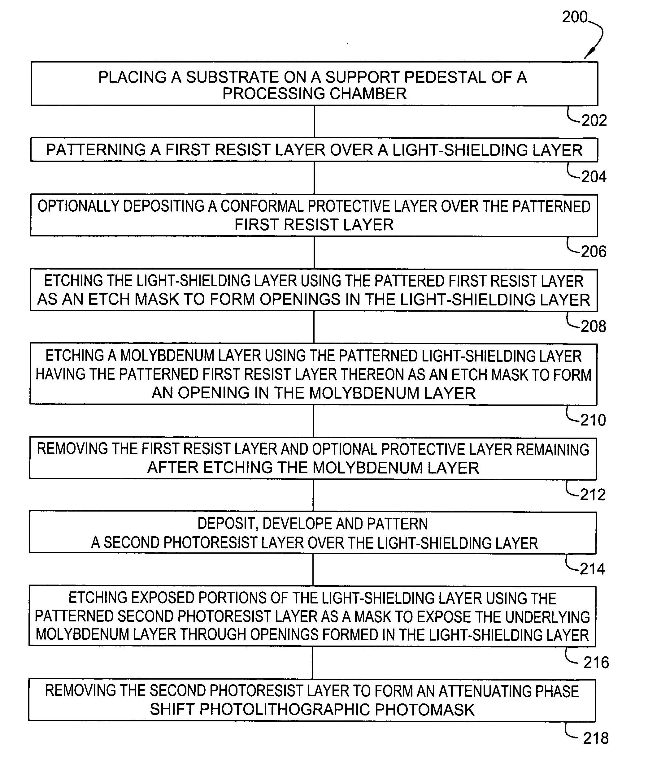
Method for etching a molybdenum layer suitable for photomask fabrication
a molybdenum layer and photomask technology, applied in insect protection, door/window protective devices, instruments, etc., can solve the problems of completely useless mask, adversely affecting performance, and use of light-attenuating material for etching
- Summary
- Abstract
- Description
- Claims
- Application Information
AI Technical Summary
Problems solved by technology
Method used
Image

Examples
Embodiment Construction
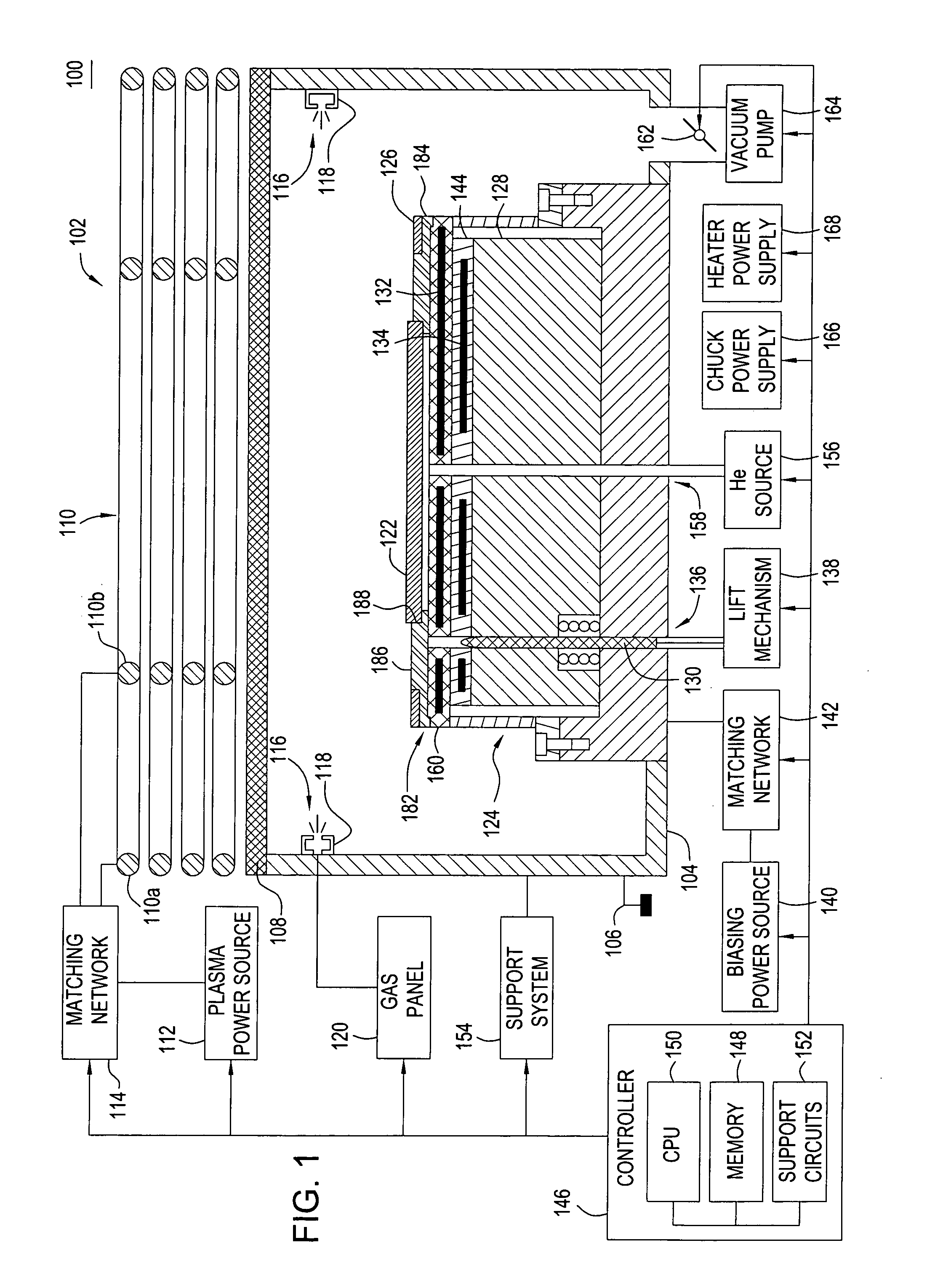
[0019]FIG. 1 depicts a schematic diagram of one embodiment of a processing chamber 100 suitable for etching molybdenum. Suitable processing chambers that may be adapted for use with the teachings disclosed herein include, for example, the Decoupled Plasma Source (DPS®) II processing chamber, or the Tetra I and Tetra II Photomask etch systems, all of which are available from Applied Materials, Inc. of Santa Clara, Calif. The particular embodiment of the processing chamber 100 shown herein is provided for illustrative purposes and should not be used to limit the scope of the invention.
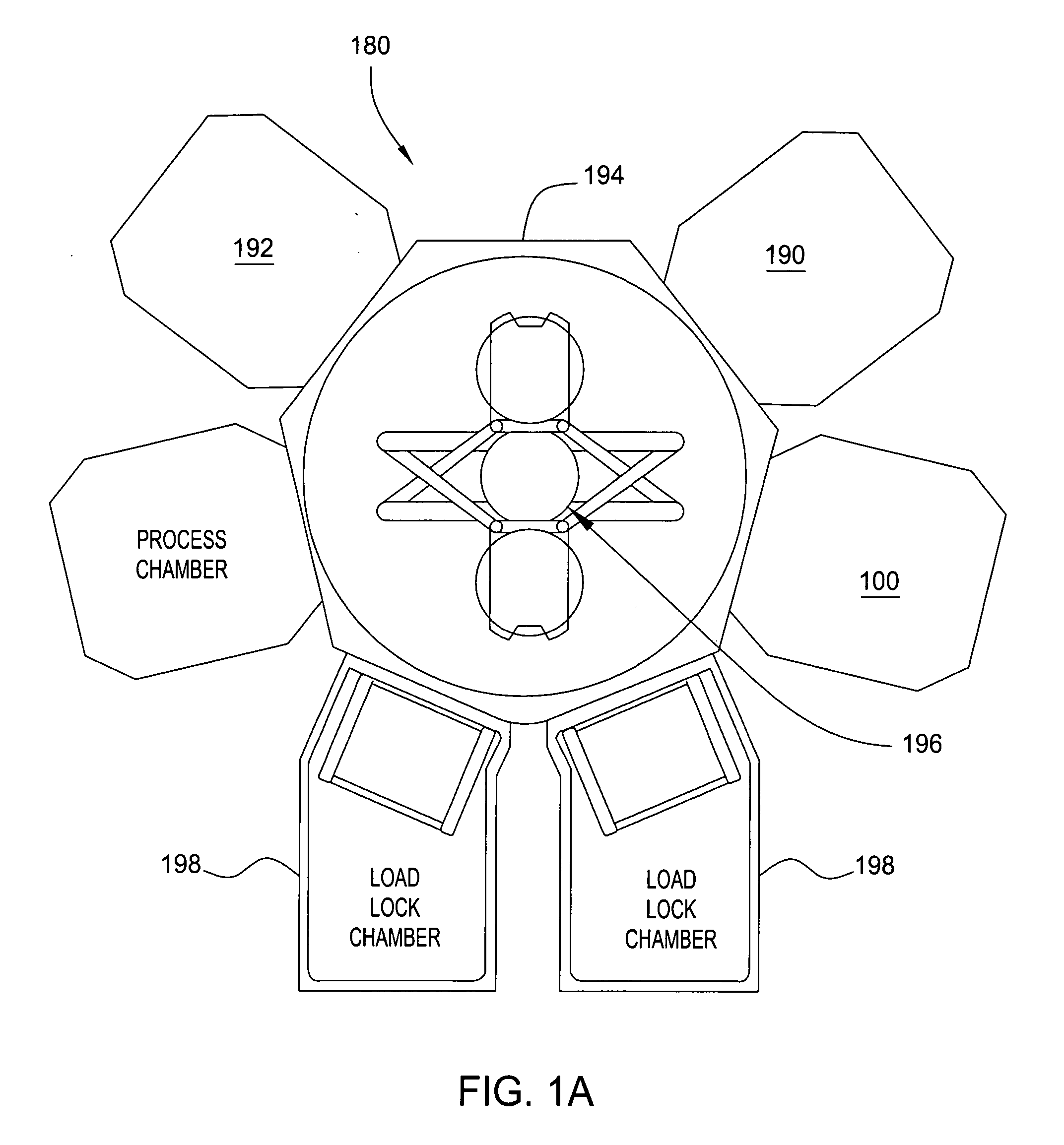
[0020] The processing chamber 100 may be part of a processing system 180 as illustrated in FIG. 1A. The processing system 180, such as, for example, a Centura® integrated semiconductor wafer processing system, also available from Applied Materials, Inc., may include a first processing chamber 192 suitable for ashing and a second chamber 194 suitable for polymer deposition. Examples of suitable ashing an...
PUM
| Property | Measurement | Unit |
|---|---|---|
| thick | aaaaa | aaaaa |
| thick | aaaaa | aaaaa |
| frequency | aaaaa | aaaaa |
Abstract
Description
Claims
Application Information
 - Generate Ideas
- Intellectual Property
- Life Sciences
- Materials
- Tech Scout
- Unparalleled Data Quality
- Higher Quality Content
- 60% Fewer Hallucinations
Browse by: Latest US Patents, China's latest patents, Technical Efficacy Thesaurus, Application Domain, Technology Topic, Popular Technical Reports.
© 2025 PatSnap. All rights reserved.Legal|Privacy policy|Modern Slavery Act Transparency Statement|Sitemap|About US| Contact US: help@patsnap.com