Plasma processing apparatus capable of controlling plasma emission intensity

a plasma processing and plasma technology, applied in the direction of electrical apparatus, basic electric elements, electric discharge tubes, etc., can solve the problems of large amount of cost in order, complex operations, and the inability of conventional plasma processing apparatuses to be applied to semiconductor manufacturing apparatus used in mass production, etc., to achieve fine devices and high precision

Inactive Publication Date: 2006-08-03
HITACHI HIGH-TECH CORP
View PDF2 Cites 119 Cited by
  • Summary
  • Abstract
  • Description
  • Claims
  • Application Information

AI Technical Summary

Benefits of technology

[0012] Since the plasma processing apparatus of the present invention is arranged with the above-described structural elements, such a plasma processing technique capable of uniformly plasma-processing very fine devices in high precision can be provided.

Problems solved by technology

However, a huge amount of cost is required in order to realize the monitoring method shown in this plasma processing apparatus, and complex operations are required when image processing operations are carried out.
As a consequence, this conventional plasma processing apparatus can be hardly applied to semiconductor manufacturing apparatus used in mass production.
However, if such a large-sized window is mounted, then the uniformity of plasma is deteriorated.
Also, deposited films are adhered and / or are scratched on the above-described window, so that these deposited films may fog up the window itself.
As a result, the window of the vacuum vessel provided in this conventional plasma processing apparatus may not be possibly used for a long time period.
However, in the conventional plasma processing apparatus of JP-A-7-86179, no care should be taken in long-term stabilities thereof when this conventional plasma processing apparatus is applied to mass production apparatus.
Also, the conventional plasma processing apparatus of JP-A-7-86179 cannot be properly used so as to manufacture semiconductor devices in very fine manners.
The electron temperatures in the plasma sources using the microwaves are increased, so that the dissociation of the processing gas is excessively progressed.
As a result, as to the long-term stability, there is such a demerit that selectivity of the mask and substrate is deteriorated.
In other words, if such a plasma source using the microwaves as shown in JP-A-7-86179 is employed in a plasma processing apparatus, then this plasma processing apparatus can hardly manufacture current semiconductor devices in very fine manners.
That is, it is practically difficult that high frequency power for generating plasma in frequency ranges from several tens of MHz to several GHz is subdivided in high precision, and a subdividing ratio of this high frequency power is control in a simple manner.
This may also increase the total cost.

Method used


Image

  • Plasma processing apparatus capable of controlling plasma emission intensity
  • Plasma processing apparatus capable of controlling plasma emission intensity
  • Plasma processing apparatus capable of controlling plasma emission intensity

Examples


Embodiment Construction

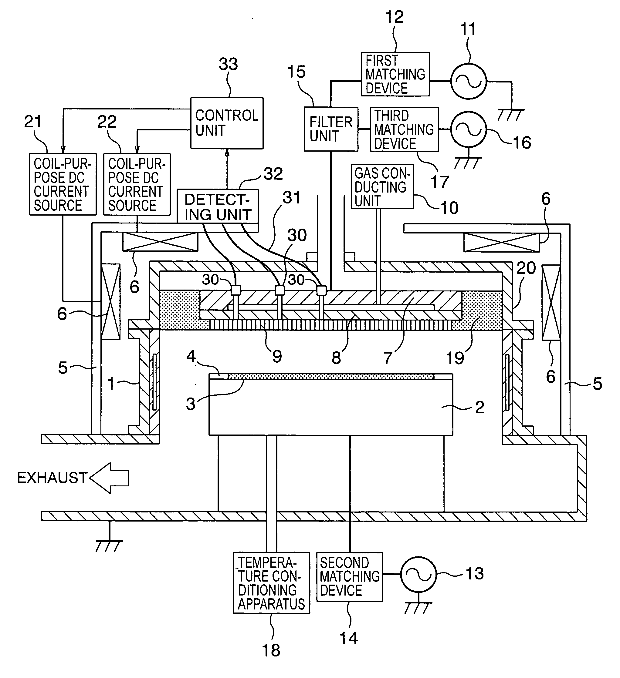
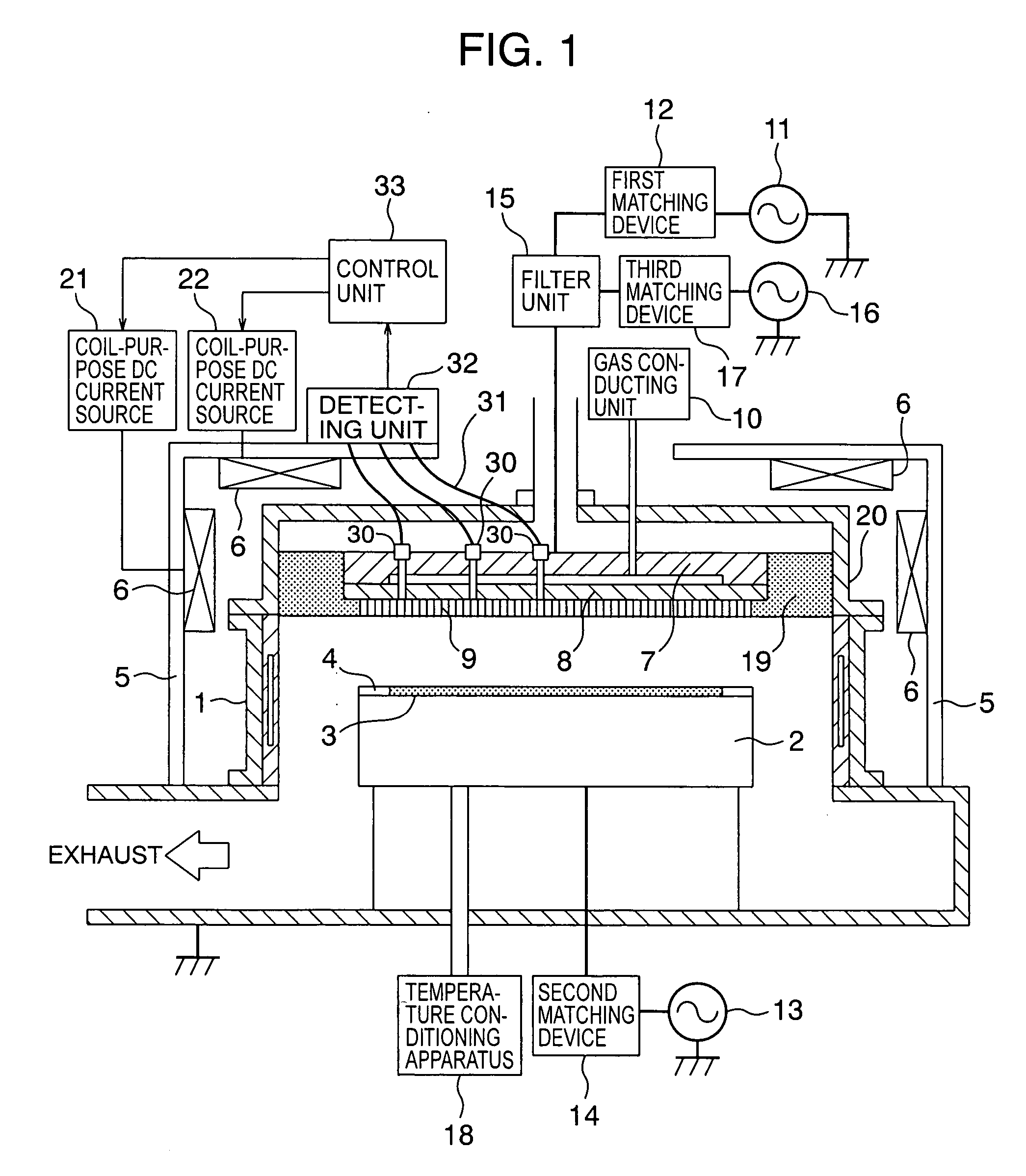
[0019] Referring now to drawings, best embodiment modes of the present invention will be described. FIG. 1 is a diagram for explaining a plasma processing apparatus according to an embodiment of the present invention. As represented in this drawing, a wafer mount-purpose stage 2, the temperature of which has been conditioned by a temperature conditioning apparatus 18, is provided inside a vacuum processing chamber 1 having a gas conducting unit 10, while the vacuum processing chamber 1 has been vacuum-exhausted, and a substantially circular shaped antenna electrode 7 is provided on a plane which is located opposite to this wafer mount-purpose stage 2, and the antenna electrode 7 is positioned parallel to the stage 2. High frequency power is supplied by a first high frequency power supply 11 via a first matching device 12 to the antenna electrode 7, and then plasma is generated by way of a mutual reaction between electromagnetic waves radiated from the antenna electrode 7 and magneti...


PUM

PropertyMeasurementUnit
diameteraaaaaaaaaa
frequencyaaaaaaaaaa
frequenciesaaaaaaaaaa

Abstract

An antenna electrode having a substantially circular shape, is arranged on a plane of a processing vessel, which is located opposite to a stage for mounting a sample within the processing vessel, and positioned parallel to the stage. An emission monitor monitors emission intensity of plasma present in at least 3 different points along a radial direction of the antenna electrode. A control unit adjusts an energizing current supplied to an external coil for forming a magnetic field within the processing vessel. The control unit adjusts the energizing current supplied to the external coil based upon the monitoring result obtained from the emission monitor so as to control the emission intensity of the plasma to become uniform emission intensity.

Description

BACKGROUND OF THE INVENTION [0001] The present invention generally relates to a plasma processing technique. More specifically, the present invention is directed to a plasma processing technique capable of uniformly processing samples. [0002] In semiconductor device manufacturing methods, plasma processing apparatus have been widely used in film forming steps and etching steps. As to these plasma processing apparatus, high-precision processing operaitons and mass production stabilities are required in correspondence with devices which should be manufactured in very fine manners. On the other hand, diameters of wafers to be processed are being enlarged in view of improvements in productivity. Nowadays, the major wafer diameter becomes 300 mm. In correspondence with large diameters of wafers, higher processing uniformity within planes of wafers is required in these plasma processing apparatus. [0003] A factor which may give the largest influence to the processing uniformity is uniform...

Claims


Application Information

Patent Timeline
Patent Type & Authority Applications(United States)
IPC IPC(8): C23F1/00
CPCH01J37/32082H01J37/32935H01J2237/3341
Inventor MAEDA, KENJIYOKOGAWA, KENETSUKANEKIYO, TADAMITSU
Owner HITACHI HIGH-TECH CORP
Why Eureka
Try Eureka