
Light emitting device and manufacture method thereof

a technology of light emitting device and manufacturing method, which is applied in the manufacture of semiconductor/solid-state devices, semiconductor devices, electrical devices, etc., can solve the problems of loss of market competitiveness, heat generated by leds, and inconvenient illumination of conventional leds, etc., and achieve the effect of facilitating the light emitting efficiency of leds

Active Publication Date: 2006-08-03
UNITED EPITAXY
View PDF3 Cites 79 Cited by
  • Summary
  • Abstract
  • Description
  • Claims
  • Application Information

AI Technical Summary

Benefits of technology

[0007] One aspect of the present invention is to provide a structure of the light emitting device which facilitates the light emitting efficiency of the LED.

Problems solved by technology

However, conventional flip-chip LEDs still require “Dicing” and “Die Bonding” for connecting and mounting the circuit board.
Therefore, the brightness of a conventional LED is not suitable for illumination purpose.
When lots of LEDs are assembled into an LED lamp to improve the brightness, the volume of the LED lamp increases accordingly, which results in the loss of its market competitiveness.
As a result, the heat generated by the LED becomes an important issue.
“Heat” seriously affects the performance of LEDs; for example, the thermal effect influences the wavelength of lights emitted from the LED, reduces the brightness of lights generated from the semiconductor device, and damages the LED device.
Therefore, how to dissipate heat generated by the high power LED become the important issue of the LEDs.
However in US Applications Nos. 2004 / 0188696 and 2004 / 0203189, it requires drilled via array with filled metal within the sub-mount wafer and thus increases the manufacturing cost.
Furthermore, it becomes complicated to flip-chip bond each chip onto the sub-mount wafer using bonding bump.

Method used


Image

  • Light emitting device and manufacture method thereof
  • Light emitting device and manufacture method thereof
  • Light emitting device and manufacture method thereof

Examples


Embodiment Construction

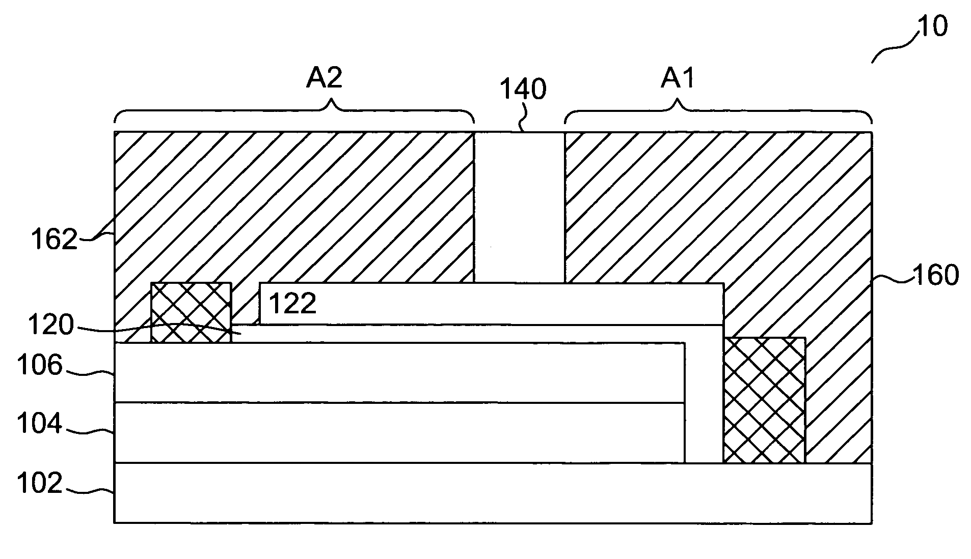
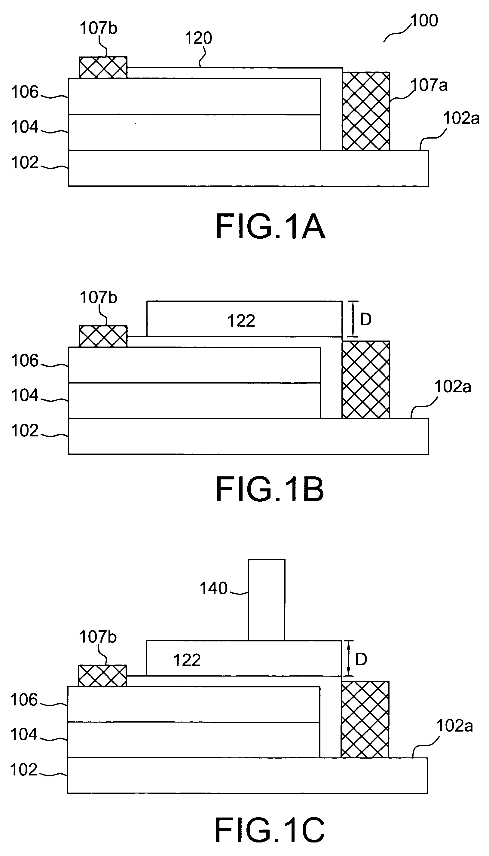
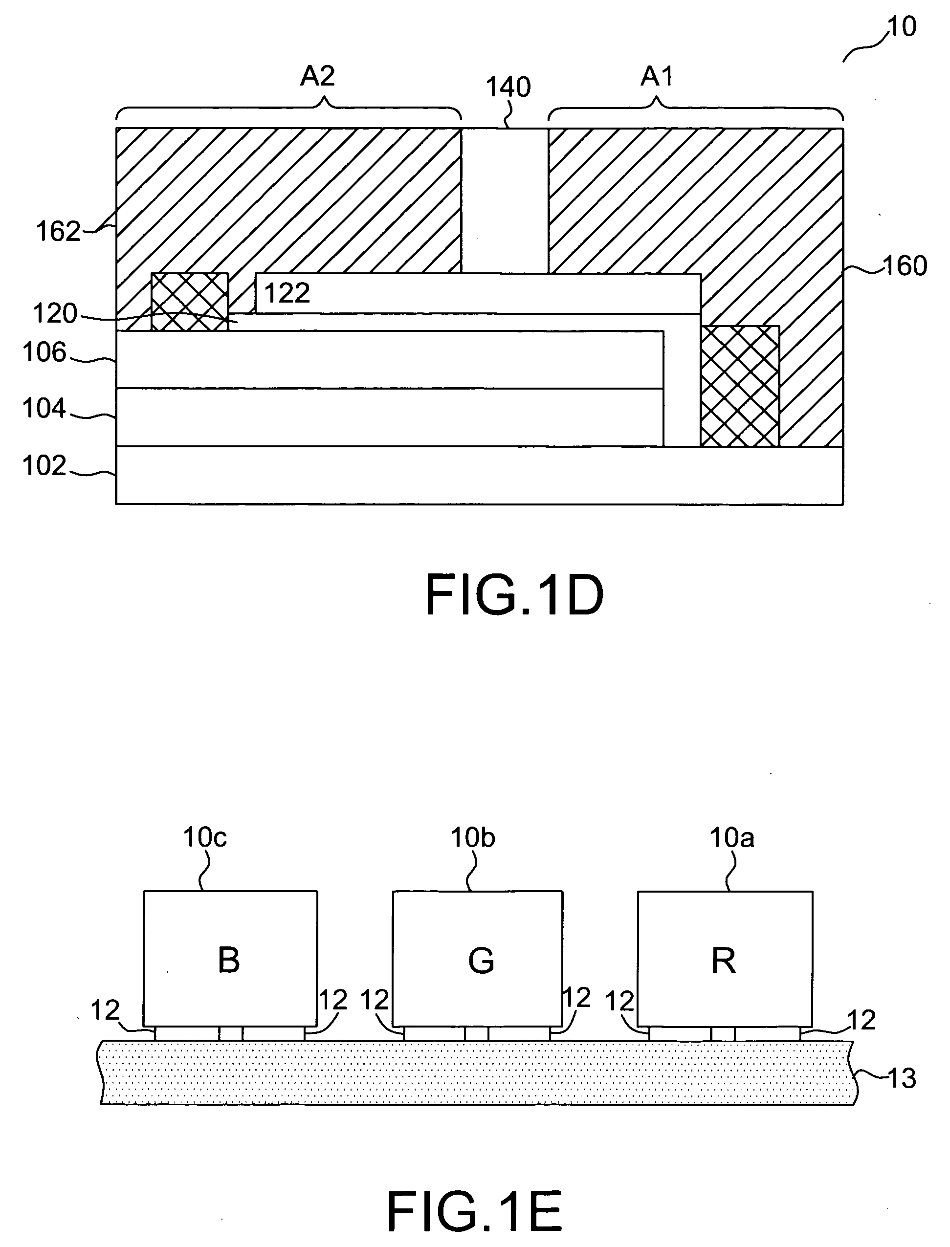
[0019]FIGS. 1A-1D illustrate the method for forming a light emitting device (LED) according to one embodiment of the present invention. Referring to FIG. 1A, at first, a light emitting structure 100 is formed. The light emitting structure 100 includes a first conductive layer 102 as a cladding layer, an active layer 104 disposed on the layer 102 as a light emitting layer, and a second conductive layer 106 disposed on the layer 104 as another cladding layer. Preferably, as shown in FIG. 1, a bonding pad 107a is disposed on an exposed portion of the layer 102, and another bonding pad 107b is disposed on the layer 106. The manufacture method and the material (e.g., Aluminum) of bonding pads 107a and 107b are well known to those skilled in the art and thus are omitted hereinafter. Furthermore, in one embodiment, the light emitting structure 100 includes a passivation layer 120 to protect the light emitting structure 100. Also, the manufacture method and the material (e.g., SiO2) of pass...


PUM


Abstract

A flip-chip LED including a light emitting structure, a first dielectric layer, a first metal layer, a second metal layer, and a second dielectric layer is provided. The light emitting structure includes a first conductive layer, an active layer, and a second conductive layer. The active layer is disposed on the first conductive layer, and the second conductive layer is disposed on the active layer. The first metal layer is disposed on the light emitting structure and is contact with the first conductive layer, and part of the first metal layer is disposed on the first dielectric layer. The second metal layer is disposed on the light emitting structure and is in contact with the second conductive layer, and part of the second metal layer is disposed on the first dielectric layer. The second dielectric layer is disposed on the first dielectric layer.

Description

CROSS REFERENCE TO RELATED APPLICATIONS [0001] This application claims priority to Taiwan Patent Application No. 094103370 entitled “Light Emitting Device and Manufacture Method thereof”, filed on Feb. 3, 2005, which is incorporated herein by reference and assigned to the assignee herein. FIELD OF INVENTION [0002] The present invention relates to a light emitting device and a method for manufacturing the same. In addition, the present invention relates to a light emitting device array and a method for manufacturing the same. BACKGROUND OF THE INVENTION [0003] For conventional light emitting device (LED) packages, a LED chip is mounted onto the sub-mount using the epoxy put thereon to form a LED element, and the process is called “Die Bonding”. Typically, the epoxy used in “Die Bonding” can be silver filled epoxy or other non-conductive resin. Then, the LED elements are assembled onto the circuit board. For a flip-chip LED, the p-type conductive layer and the n-type conductive layer ...

Claims


Application Information

Patent Timeline
Patent Type & Authority Applications(United States)
IPC IPC(8): H01L33/00H01L33/32H01L27/15H01L33/38H01L33/62H01L33/64
CPCH01L25/0753H01L33/385H01L33/46H01L33/62H01L2933/0016H01L33/36H01L33/38H01L33/387H01L2924/0002H01L2924/00
Inventor TU, CHUAN-CHENGWU, JEN-CHAUSHIEH, YUH-REN
Owner UNITED EPITAXY
Features
  • Generate Ideas
  • Intellectual Property
  • Life Sciences
  • Materials
  • Tech Scout
  • Unparalleled Data Quality
  • Higher Quality Content
  • 60% Fewer Hallucinations
Learn More