Non-volatile memory and manufacturing and operating method thereof

a technology of non-volatile memory and manufacturing method, which is applied in the direction of semiconductor devices, basic electric elements, electrical apparatus, etc., can solve the problems of leakage current and affecting device reliability, abnormal electrical punch-through of the channel underneath the memory cell with a higher frequency, and achieve the effect of increasing the overall level of device integration

Active Publication Date: 2006-08-03
POWERCHIP SEMICON MFG CORP
View PDF24 Cites 35 Cited by
  • Summary
  • Abstract
  • Description
  • Claims
  • Application Information

AI Technical Summary

Benefits of technology

[0011] Accordingly, at least one objective of the present invention is to provide a non-volatile memory and manufacturing and operating method thereof. The non-volatile memory has no device isolation structure between various memory cell arrays and no contact and no doped region between various memory cells so that the overall level of integration of the device can be increased.

Problems solved by technology

On the other hand, because doped polysilicon is used to fabricate the floating gates, any defects in the tunneling oxide layer under the floating gate can easily produce a leakage current and affect the reliability in the device.
As a result, abnormal electrical punch-through of the channel underneath the memory cell occurs with higher frequency.

Method used


Image

  • Non-volatile memory and manufacturing and operating method thereof
  • Non-volatile memory and manufacturing and operating method thereof
  • Non-volatile memory and manufacturing and operating method thereof

Examples


Embodiment Construction

[0050] Reference now is made in detail to the present embodiments of the invention, examples of which are illustrated in the accompanying drawings. Wherever possible, the same reference numbers are used in the drawings and the description to refer to the same or like parts.

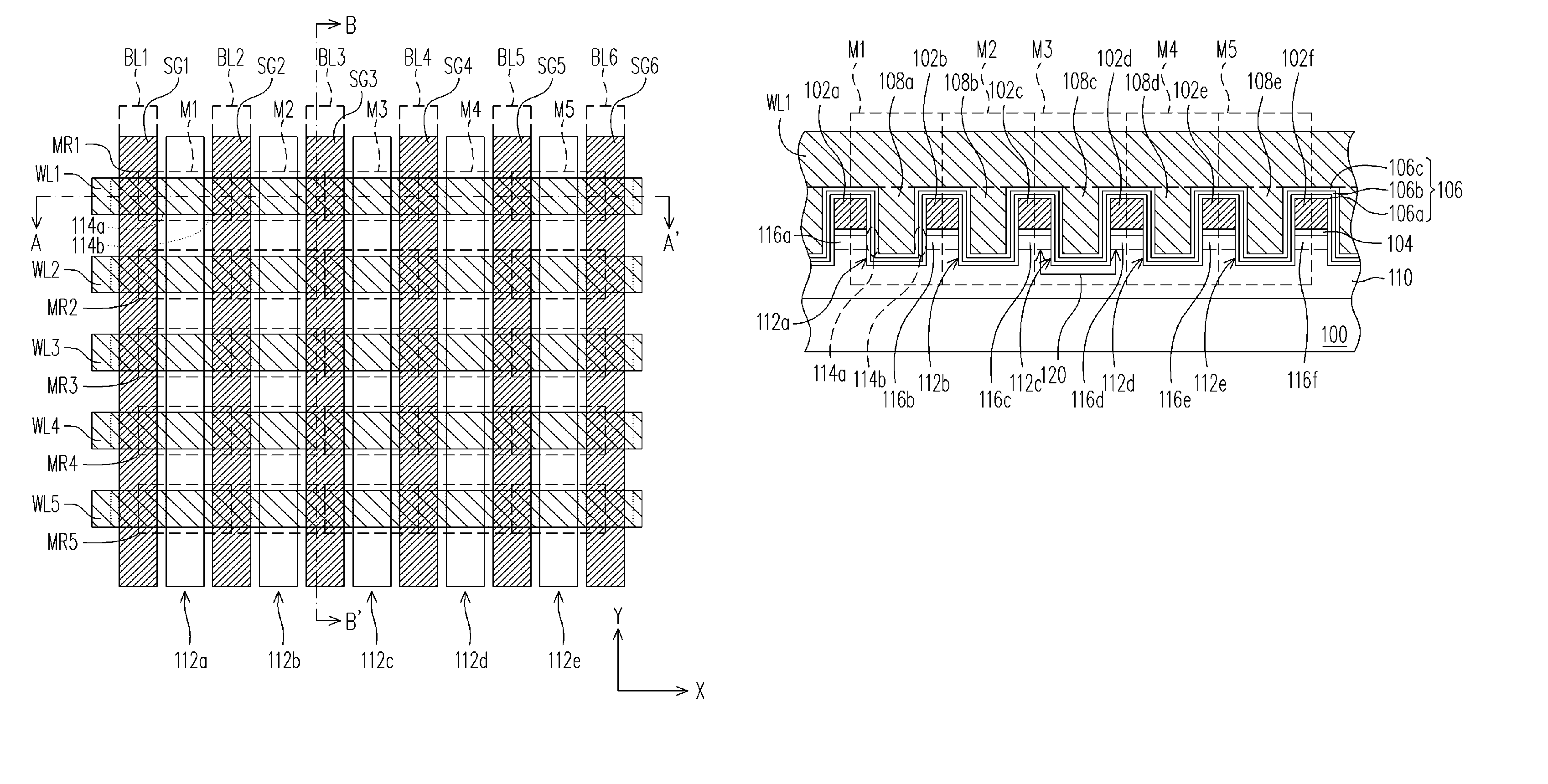
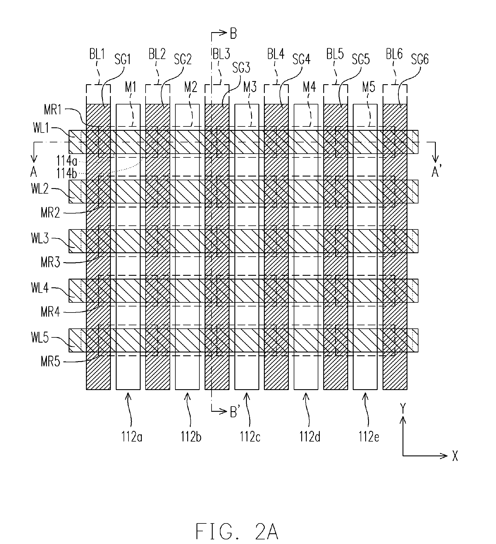
[0051]FIG. 2A is a top view of a non-volatile memory according to one embodiment of the present invention. FIG. 2B is a cross-sectional view along line A-A′ of FIG. 2A. FIG. 2C is a cross-sectional view along line B-B′ of FIG. 2A. As shown in FIG. 2A, the non-volatile memory array of the present invention includes a substrate 100, a plurality of memory cell arrays MR1·MR5, a plurality of word lines WL1˜WL5, a plurality of select gate lines SG1˜SG6, and a plurality of bit lines BL1˜BL6.

[0052] The memory cell arrays MR1˜MR5 are arranged to form a memory array. The word lines WL1˜WL 5 are coupled to the control gates respectively in the same row of memory cells. The word lines WL1˜WL5 are arranged in parallel to ea...


PUM


Abstract

A non-volatile memory is provided. A substrate having a plurality of trenches and a plurality of select gates is provided. The trenches are arranged in parallel and extend in a first direction. Each of the select gates is disposed on the substrate between two adjacent trenches respectively. A plurality of select gate dielectric layers are disposed between the select gates and the substrate. A plurality of composite layers are disposed over the surface of the trenches and each composite layer has a charge trapping layer. A plurality of word lines are arranged in parallel in a second direction, wherein each of the word lines fills the trenches between adjacent select gates and is disposed over the composite layers.

Description

CROSS-REFERENCE TO RELATED APPLICATION [0001] This application claims the priority benefit of Taiwan application serial no. 94102849, filed on Jan. 31, 2005. All disclosure of the Taiwan application is incorporated herein by reference. BACKGROUND OF THE INVENTION [0002] 1. Field of the Invention [0003] The present invention relates to a semiconductor device. More particularly, the present invention relates to a non-volatile memory and manufacturing and operating method thereof. [0004] 2. Description of the Related Art [0005] Among the various types of non-volatile memory products, electrically erasable programmable read only memory (EEPROM) is a memory device that has been widely used inside most personal computer systems and electronic equipment. In an EEPROM, data can be stored, read out or erased from the EEPROM numerous times and any stored data is retained even after power is cut off. [0006] Typically, the floating gate and the control gate of an EEPROM cell is fabricated using...

Claims


Application Information

Patent Timeline
Patent Type & Authority Applications(United States)
IPC IPC(8): H01L29/94
CPCH01L27/115H01L27/11521H01L27/11568H10B69/00H10B41/30H10B43/30
Inventor WONG, WEI-ZHEYANG, CHING-SUNG
Owner POWERCHIP SEMICON MFG CORP
Why Eureka
Try Eureka