Display device

a display device and display technology, applied in the field of display devices, can solve the problems of not maintaining a sufficient color reproduction range over wide view angles, device does not envisage, and cannot obtain a sufficient color reproduction range to display, so as to reduce external light reflection, improve contrast, and reduce luminance

Inactive Publication Date: 2006-08-10
SONY CORP
View PDF3 Cites 57 Cited by
  • Summary
  • Abstract
  • Description
  • Claims
  • Application Information

AI Technical Summary

Benefits of technology

[0012] Another object of the invention is to provide a spontaneous emission type display device that can reduce reflection of external light and thereby improves the contrast without inviting a decrease in luminance.

Problems solved by technology

Therefore, with a display apparatus made by using such organic EL devices for color representation, it was impossible to obtain a sufficient color reproduction range enough to display, for example, TV images.
However, the organic EL device does not envisage the dependency of the view angle in its design, and could not maintain a sufficient color reproduction range over wide view angles.
Moreover, the organic EL device, in problem, had to optimize the cavity structure for light h of each color to be extracted, and required an additional effort for it.
Although display devices with this configuration could prevent reflection of external light other than emitted light, they cannot prevent reflection of external light outside the wavelength ranges of the emission colors of respective pixels.

Method used


Image

  • Display device
  • Display device
  • Display device

Examples


fourth embodiment

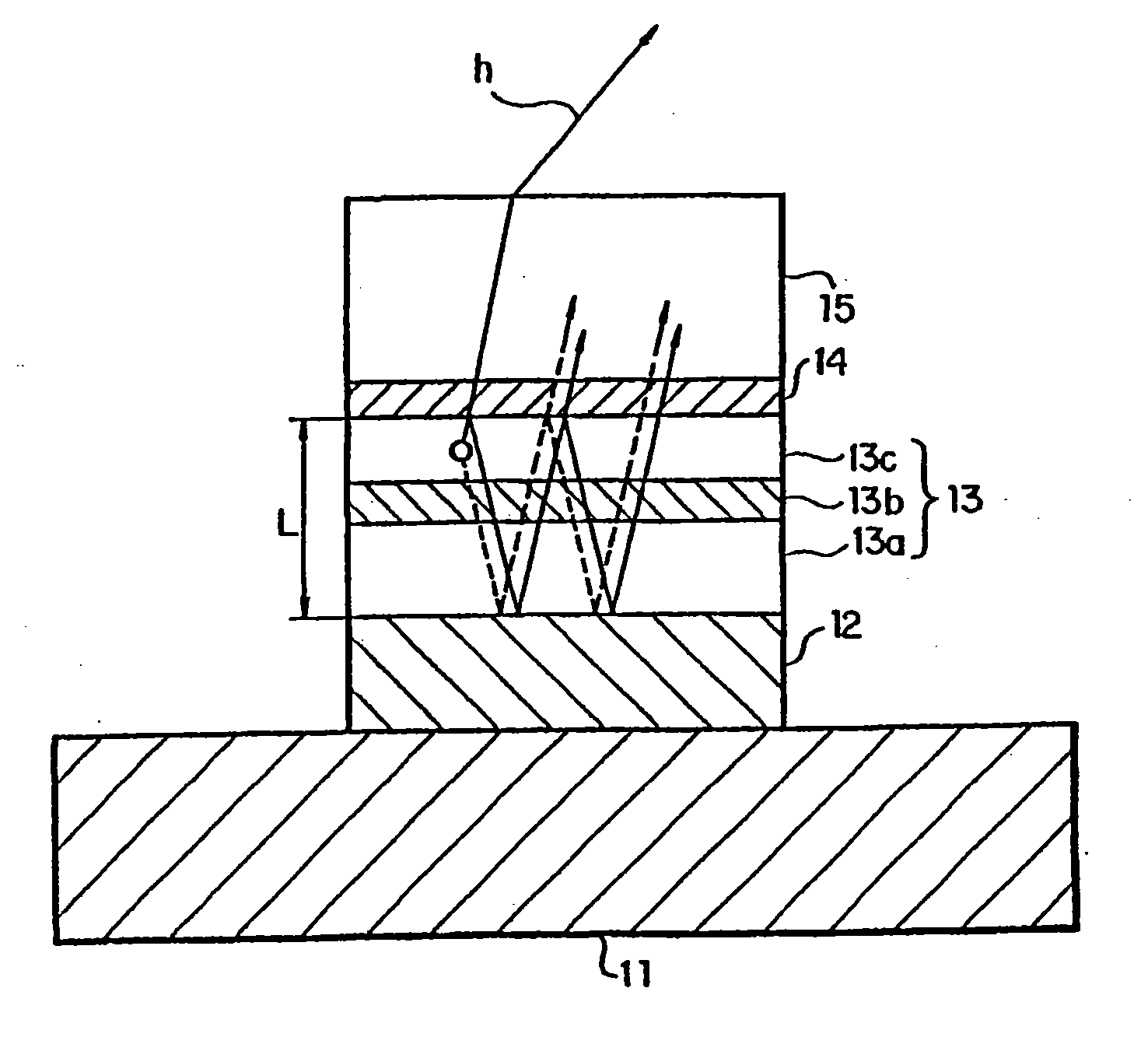
[0088]FIG. 19 is a cross-sectional view that shows a central part of an organic EL device according to the fourth embodiment of the invention. The organic EL device shown in FIG. 19 includes a color filter in addition to the top surface emission type organic EL device according to the first embodiment shown in FIG. 4. More specifically, the first electrode 12 as the reflection layer, organic layer 13 and semitransparent reflection layer 14 make up the cavity structure, with the organic layer 13 as the cavity portion, and a color filter 20 is disposed on the semitransparent reflection layer 14 via the second electrode (transparent electrode) 15 and the passivation film 16.

[0089] Let the color filter 20 be configured to transmit only light h near the peak wavelength λ of a spectrum to be extracted from the organic EL device. That is, a device for emitting light in the red (R) region has a color filter 20R that transmits light exclusively in the red (R) region, a device for emitting l...


PUM


Abstract

In an organic EL device having a first electrode of a light reflective material, organic layer including an organic light emitting layer, semitransparent reflection layer, and second electrode of a transparent material that are stacked sequentially, and so configured that the organic layer functions as a cavity portion of a cavity structure, light that resonates in a certain spectral width (wavelength λ) is extracted by so configuring that optical path length L becomes minimum in a range satisfying (2L)/λ+Φ((2π)=m (m is an integer) where the phase shift produced in light generated in the organic light emitting layer when reflected by opposite ends of the cavity portion is Φ radians, L is optical path length of the cavity portion, and λ is the peak wavelength of the spectrum of part of light to be extracted.

Description

RELATED APPLICATION DATA [0001] This application is a continuation of U.S. patent application Ser. No. 09 / 889,532, filed Oct. 2, 2001, which is incorporated herein by reference to the extent permitted by law. This application claims the benefit of priority to International Patent Application No. PCT / JP00 / 08233, filed Nov. 22, 2000, which is also incorporated herein by reference to the extent permitted by law.FIELD OF THE INVENTION [0002] This invention relates to a display device and, more particularly, to a spontaneous emission-type display device such as organic electroluminescense device. BACKGROUND OF THE INVENTION [0003] A device using electroluminescense of an organic material (hereinafter called “organic EL device”) is made of an organic layer in which an organic hole transport layer, or organic light emitting layer, interposed between a first electrode and a second electrode, and it is remarked as a spontaneous emission type display device capable of high-luminance emission ...

Claims


Application Information

Patent Timeline
Patent Type & Authority Applications(United States)
IPC IPC(8): H01L51/52H05B33/02H01L27/32H01L33/10H01L33/26H01L33/42H01L33/44
CPCH01L27/322H01L51/5265H01L2251/5315H05B33/22Y10S428/917H10K59/38H10K50/852H10K2102/3026H05B33/00
Inventor YAMADA, JIROSASAOKA, TATSUYAHIRANO, TAKASHI
Owner SONY CORP
Why Eureka
Try Eureka