High performance CMOS NOR predecode circuit

Inactive Publication Date: 2006-08-10
IBM CORP
View PDF5 Cites 9 Cited by
  • Summary
  • Abstract
  • Description
  • Claims
  • Application Information

AI Technical Summary

Benefits of technology

[0007] An object of this invention is the provision of a

Problems solved by technology

As will be appreciated by those skilled in the art, the performance of a

Method used


Image

  • High performance CMOS NOR predecode circuit
  • High performance CMOS NOR predecode circuit
  • High performance CMOS NOR predecode circuit

Examples


Example

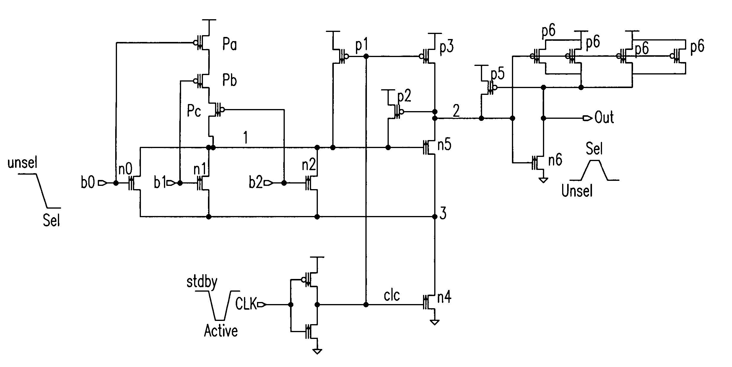
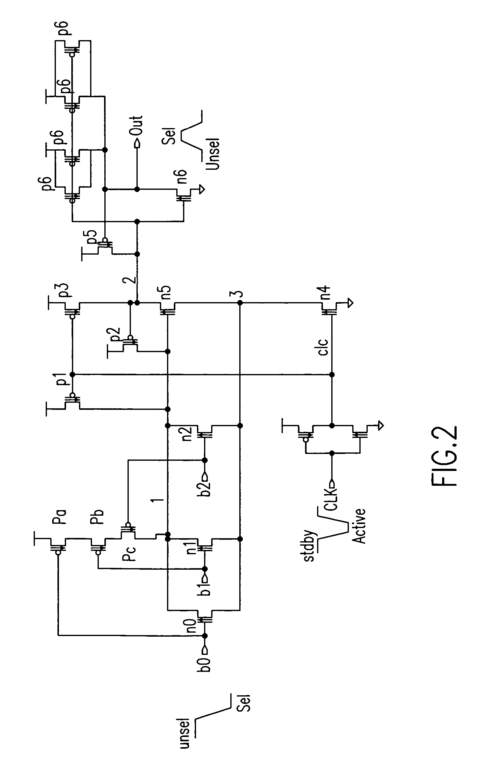
[0012] Referring now to FIG. 2, three PFETs (Pa, Pb, and Pc) coupled in a series stack between the input node 1 and the decoder supply voltage Vdd. The gates of Pa, Pb and Pc are coupled respectively to the decoder inputs b1, b2, and b3. Thus it will be appreciated, that when all three inputs are selected, the transistors of the series stack Pa, Pb, and Pc are all forwardly biased and connect node 1 to the supply voltage Vdd, thus holding node 1 high, and reducing the dip in node 1 caused by the capacitive coupling in transistors P2 and N5 described above. With the PFET stack added, the input stage (consisting of decoding devices Pa, Pb, Pc and n0-n2) now fully forms a 3-input NOR decode structure to drive the rest of the decoder circuit, which operates in dynamic fashion. As a result, the noise glitch seen on the decoding node (node 1) is much reduced. The decoder's switching performance is greatly improved.

[0013] While the preferred embodiment of the invention has been described,...


PUM


Abstract

A CMOS decoder with an FET stack coupled to the input node so that when all the inputs are selected, the FET stack is conducting and initially holds the value on the input node, and prevents dipping of the input node voltage.

Description

CROSS REFERENCE TO RELATED APPLICATIONS [0001] This application contains subject matter that is related to the subject matter of the following co-pending applications, each of which is assigned to the same assignee as this application, International Business Machines Corporation of Armonk, N.Y., and is filed concurrently herewith. Each of the below listed applications is hereby incorporated herein by reference. High Speed Domino Bit Line Interface Early Read and Noise Suppression, Attorney Docket POU9 2004 0217; Global Bit Select Circuit With Dual Read and Write Bit Line Pairs, Attorney Docket POU9 2004 0214; Local Bit Select Circuit With Slow Read Recovery Scheme, Attorney Docket POU9 2004 0224; Global Bit Line Restore Timing Scheme and Circuit, Attorney Docket POU9 2004 1234; Local Bit Select With Suppression, Attorney Docket POU9 2004 0246. BACKGROUND OF THE INVENTION [0002] 1. Field of the Invention [0003] This invention relates to an improved decode circuit using CMOS implement...

Claims


Application Information

Patent Timeline
IPC IPC(8): G11C8/00
CPCG11C8/10
Inventor CHAN, YUEN H.SRINIVASAN, UMAWADHWA, JATINDER K.
Owner IBM CORP
Why Eureka
Try Eureka