

Nitride semiconductor device
- Summary
- Abstract
- Description
- Claims
- Application Information
AI Technical Summary
Benefits of technology
Problems solved by technology
Method used
Image

Examples
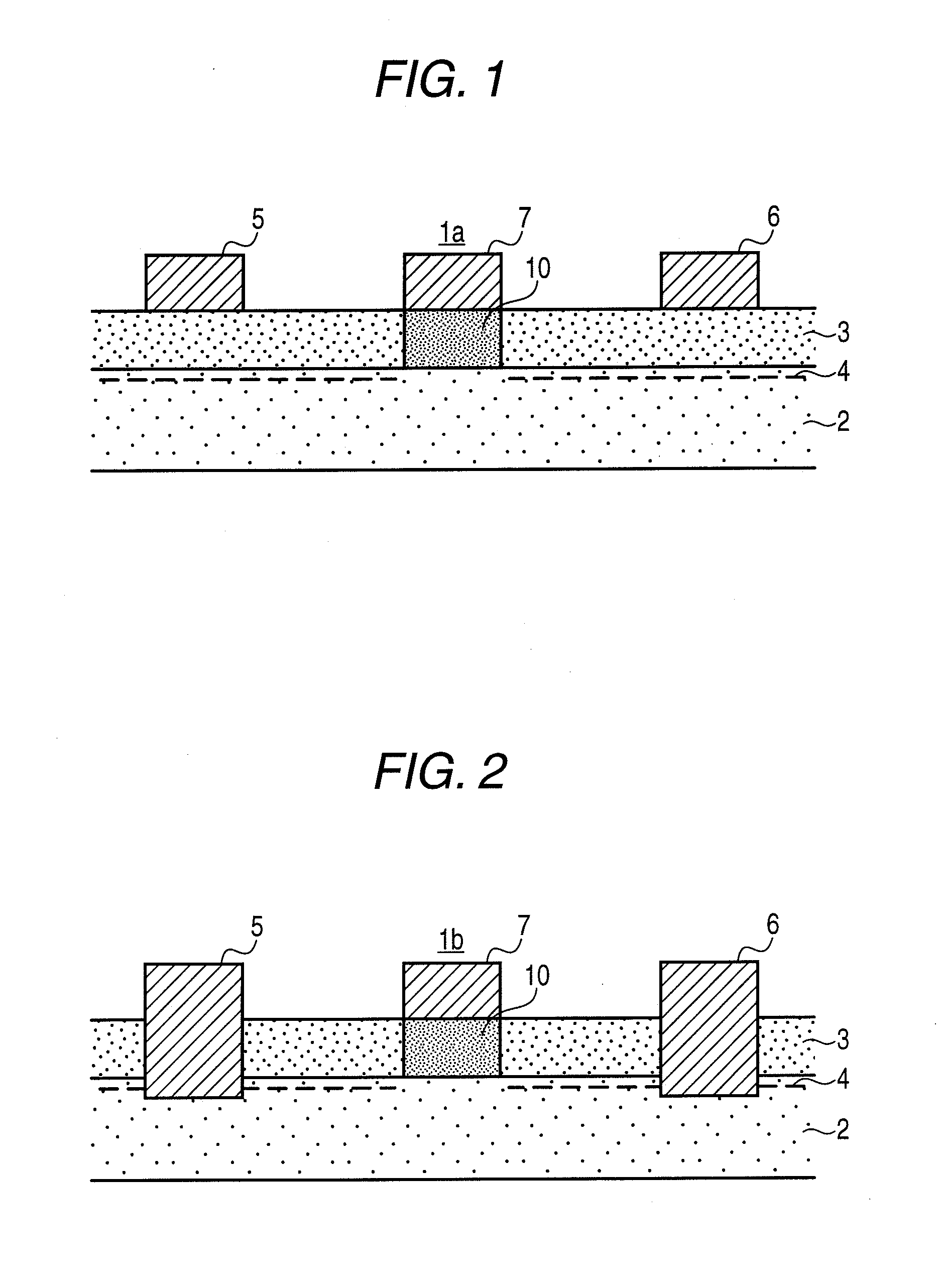
first embodiment
[0016]A HEMT 1a according to the invention shown in FIG. 1 includes a channel layer 2 (an example of a first nitride semiconductor layer) formed on a single-crystal silicon semiconductor substrate (not shown), a barrier layer 3 (an example of a second nitride semiconductor) formed on the channel layer 2, a source electrode 5 formed on the barrier layer 3, a drain electrode 6 formed on the barrier layer 3 and separated from the source electrode 5, a gate layer 10 (an example of a third nitride semiconductor layer) formed so as to abut on the channel layer 2 and extend through the barrier layer 3 between the drain electrode 6 and the source electrode 5 on the channel layer 2, and a gate electrode 7 formed on the gate layer 10. In other words, combination of the channel layer 2 and the barrier layer 3 can be an example of a main semiconductor region.
[0017]The channel layer 2 is formed, for example, of AlxGa1-xN (00.3Ga0.7N layer of 0.5 to 2.0 μm. Also, the barrier layer 3 is formed of ...
second embodiment
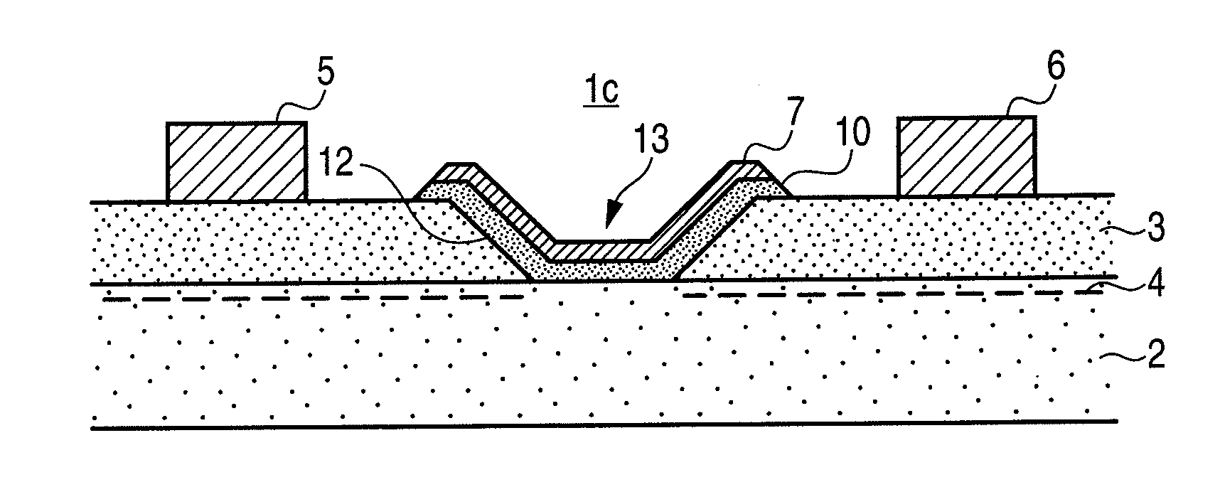
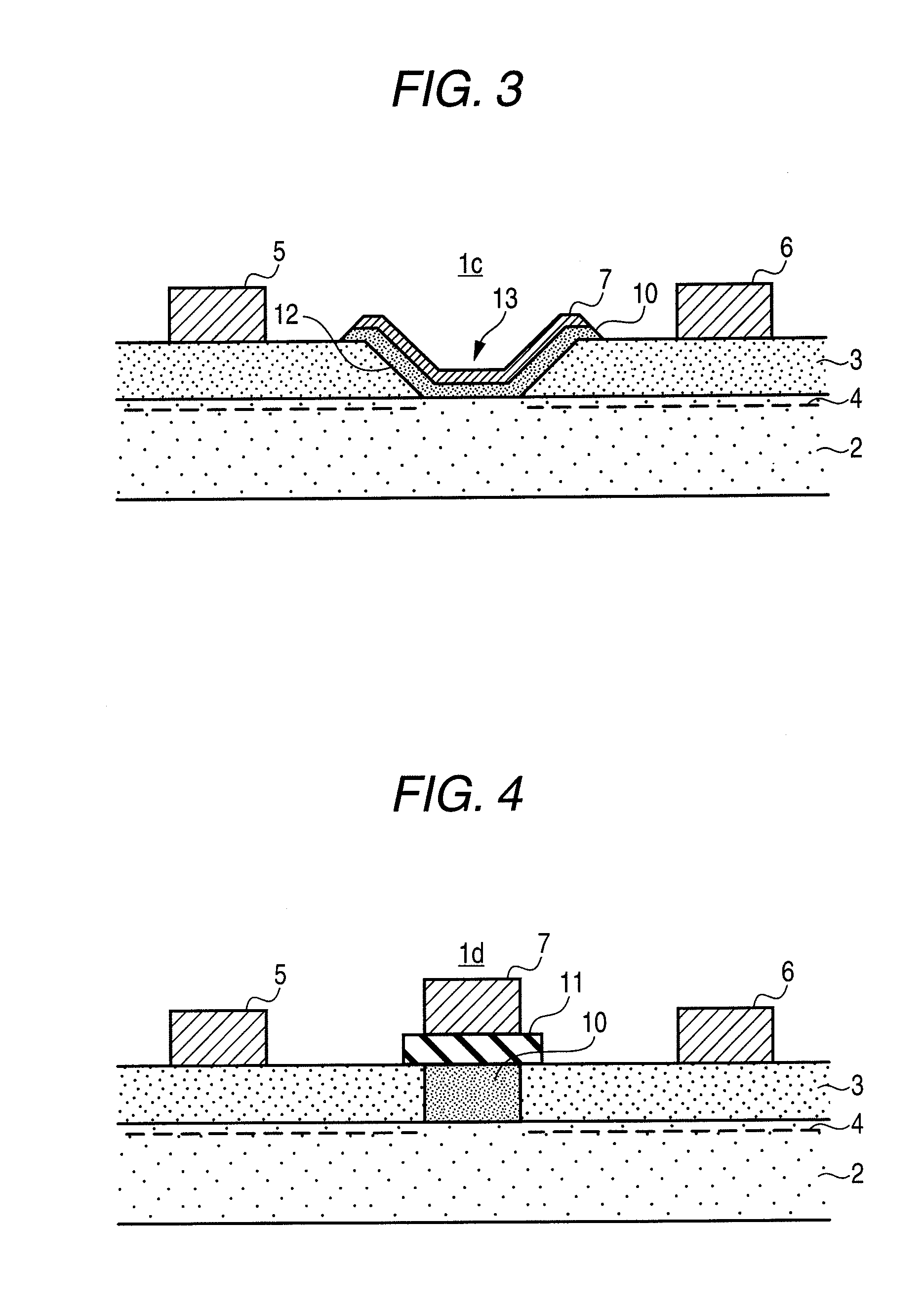
[0031]Next, a HEMT 1d according to the invention shown in FIG. 4 will be described. In FIG. 4, the description is omitted by assigning the same numerals to substantially the same elements as FIG. 1.
[0032]The HEMT 1d according to the present embodiment differs from the first embodiment in that a compound layer 11 is formed between a gate layer 10 and a gate electrode 7, and others are formed similarly.
[0033]The compound layer 11 in the embodiment includes an insulator such as silicon oxide (SiO, SiO2), silicon nitride (SiN), aluminum oxide (Al2O3) or hafnium oxide (HfO), and is formed by performing a plasma CVD method etc. after the gate layer 10 is formed. For example, the compound layer 11 in the embodiment is obtained by forming an SiO2 layer of 10 to 100 nm.
[0034]According to the HEMT 1d formed thus, an effect similar to the HEMT 1a according to the first embodiment of the invention is obtained. Also, a gate leakage current can be reduced by forming the compound layer 11 between ...
PUM
 Abstract
Description
Claims
Application Information