Silicon phosphor electroluminescence device with nanotip electrode

a technology of nano-tip electrodes and electroluminescence devices, which is applied in the field of integrated circuit (ic) fabrication, can solve problems such as poor light generation efficiency, and achieve the effect of high field

Inactive Publication Date: 2006-08-17
SHARP KK
View PDF2 Cites 12 Cited by
  • Summary
  • Abstract
  • Description
  • Claims
  • Application Information

AI Technical Summary

Problems solved by technology

For silicon devices, the light generation efficiency is known to be poor and the photon energy is predominantly around 2 eV.
However, these devices are fabricated on materials that are typically not compatible with silicon, for example type III-V materials such as InGaN, AlGaAs, GaAsP, GaN, and GaP.

Method used


Image

  • Silicon phosphor electroluminescence device with nanotip electrode
  • Silicon phosphor electroluminescence device with nanotip electrode
  • Silicon phosphor electroluminescence device with nanotip electrode

Examples


Embodiment Construction

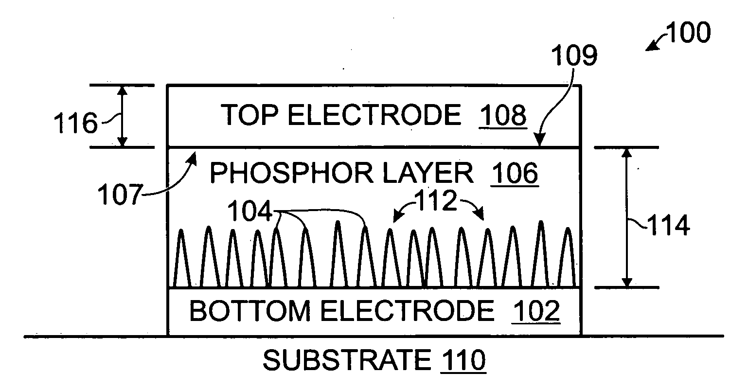
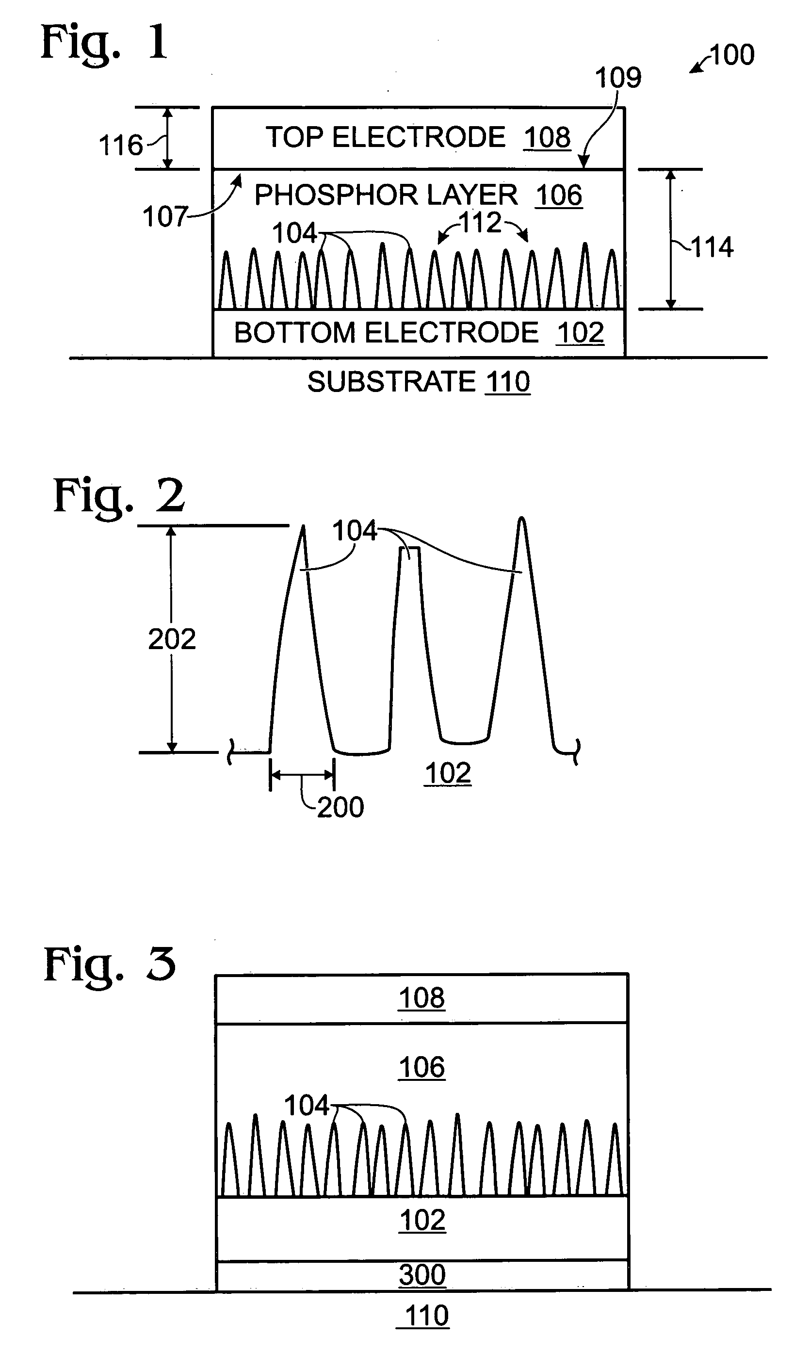
[0026]FIG. 1 is a partial cross-sectional view of a nanotip electrode electroluminescence (EL) device. The EL device 100 comprises a bottom electrode 102 with nanotips 104. A silicon (Si) phosphor layer 106 is adjacent the nanotips 104. A transparent top electrode 108 overlies the Si phosphor layer 106. The Si phosphor layer 106 is interposed between the top electrode 108 and the bottom electrode 102.

[0027] As used herein, the word “nanotip” is not intended to be limited to any particular physical characteristics, shapes, or dimensions. The nanotips may alternately be known as nanorods, nanotubes, or nanowires. In some aspects (not shown), the nanotips may form a hollow structure. In other aspects (not shown), the nanotips may be formed with a plurality of tips ends. Although the nanotips 104 are shown substantially vertical, and therefore, perpendicular to the (horizontal) surfaces of the bottom electrode 102, the nanotips are not limited to any particular orientation with respect...


PUM

PropertyMeasurementUnit
sizeaaaaaaaaaa
heightaaaaaaaaaa
partial pressureaaaaaaaaaa

Abstract

An electroluminescence (EL) device and a method are provided for fabricating said device with a nanotip electrode. The method comprises: forming a bottom electrode with nanotips; forming a Si phosphor layer adjacent the nanotips; and, forming a transparent top electrode. The Si phosphor layer is interposed between the bottom and top electrodes. The nanotips may have a tip base size of about 50 nanometers, or less, a tip height in the range of 5 to 50 nm, and a nanotip density of greater than 100 nanotips per square micrometer. Typically, the nanotips are formed from iridium oxide (IrOx) nanotips. A MOCVD process forms the Ir bottom electrode. The IrOx nanotips are grown from the Ir. In one aspect, the Si phosphor layer is a SRSO layer. In response to an SRSO annealing step, nanocrystalline SRSO is formed with nanocrystals having a size in the range of 1 to 10 nm.

Description

BACKGROUND OF THE INVENTION [0001] 1. Field of the Invention [0002] This invention generally relates to integrated circuit (IC) fabrication and, more particularly, to an electroluminescence device made using a silicon phosphor and an electrode with nanotips. [0003] 2. Description of the Related Art [0004] The generation of light from semiconductor devices is possible, regardless of whether the semiconductor material forms a direct or indirect bandgap. High field reverse biased p-n junctions create large hot carrier populations that recombine with the release of photons. For silicon devices, the light generation efficiency is known to be poor and the photon energy is predominantly around 2 eV. The conversion of electrical energy to optical photonic energy is called electroluminescence (EL). Efficient EL devices have been made that can operate with small electrical signals, at room temperature. However, these devices are fabricated on materials that are typically not compatible with s...

Claims


Application Information

Patent Timeline
Patent Type & Authority Applications(United States)
IPC IPC(8): H01L27/15
CPCH05B33/145
Inventor HSU, SHENG TENGZHANG, FENGYANSTECKER, GREGORY M.BARROWCLIFF, ROBERT A.
Owner SHARP KK
Why Eureka
Try Eureka