Semiconductor light emitting device, light emitting module and lighting apparatus

Active Publication Date: 2006-08-17
PANASONIC CORP
View PDF12 Cites 191 Cited by
  • Summary
  • Abstract
  • Description
  • Claims
  • Application Information

AI Technical Summary

Benefits of technology

[0017] The first object can be achieved by a semiconductor light emitting device including a substrate; a first light emitting member that is formed on the substrate in an epitaxial growth step of a wafer fabrication process; an electrically conductive pattern that is formed on the substrate in a wiring step of the wafer fabrication process; and a second light emitting member that is separately formed and then mounted on the electrically conductive pattern. Here, the second light emitting member emits light of a different color from the first light emitting member. According to this construction, the second light emitting member is mounted on the electrically conductive pattern that is formed in the wiring step. This enables high-precision

Problems solved by technology

Accordingly, the white LED is not suitable as an alternative light source for halogen lamps, which have a color temperature of 3000 K.
Since a red phosphor only has a low color conversion efficiency, these white LEDs have not yet been put into practical use in any technical fields.
These white LEDs have not yet been put into practical use for lighting because of large unevenness of color that is caused for the following reason.
On the printed-wiring board, the LED chips are inevitably arranged at large intervals, due to tec

Method used


Image

  • Semiconductor light emitting device, light emitting module and lighting apparatus
  • Semiconductor light emitting device, light emitting module and lighting apparatus
  • Semiconductor light emitting device, light emitting module and lighting apparatus

Examples


Embodiment Construction

[0039] The following describes an embodiment of the present invention with reference to the attached drawings.

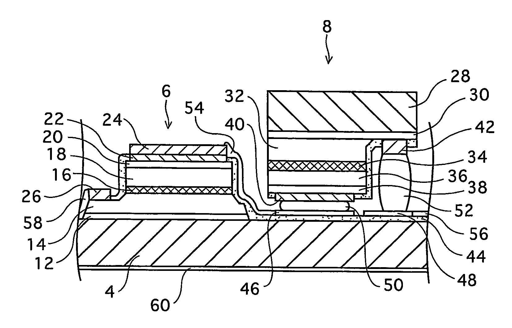
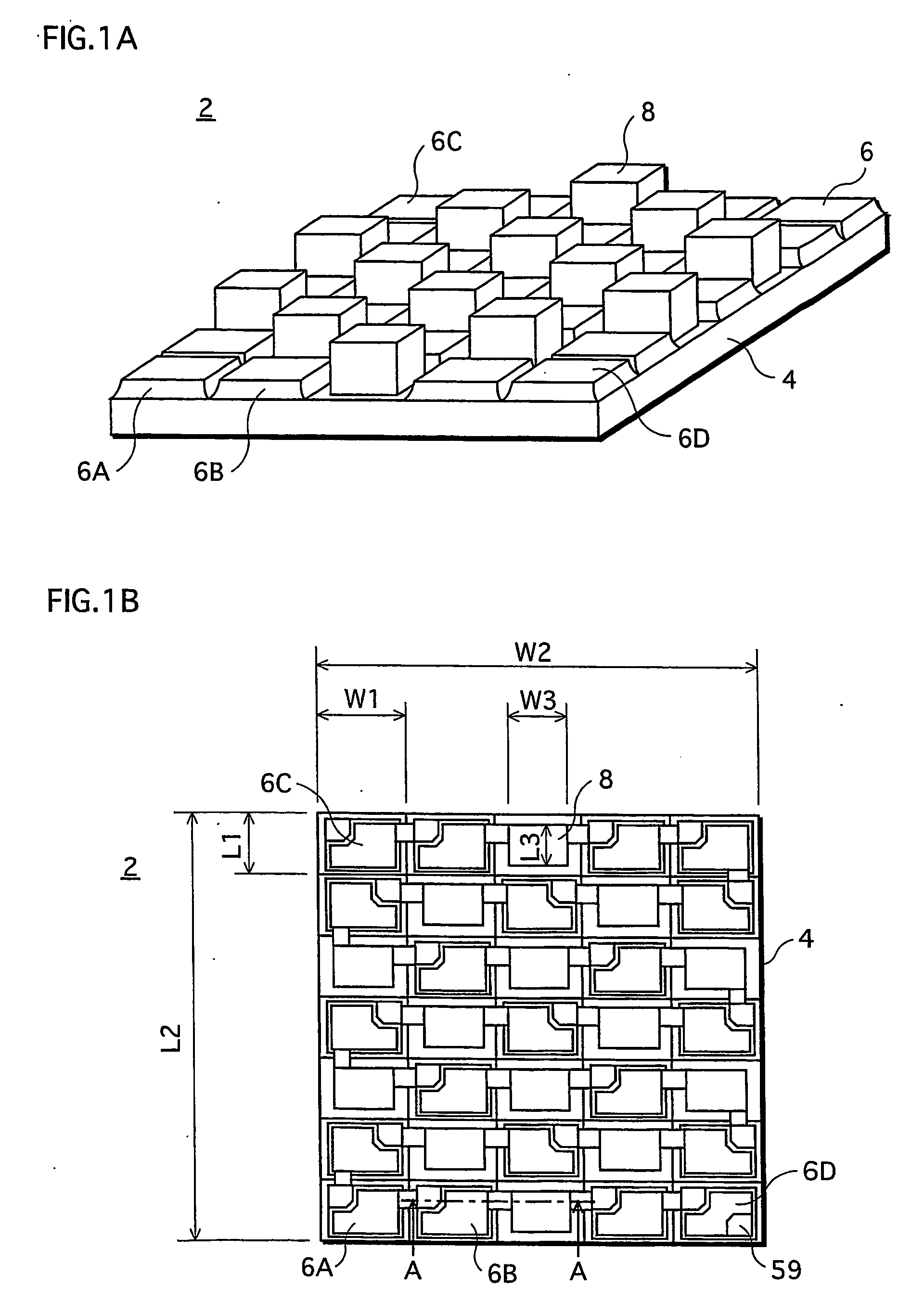
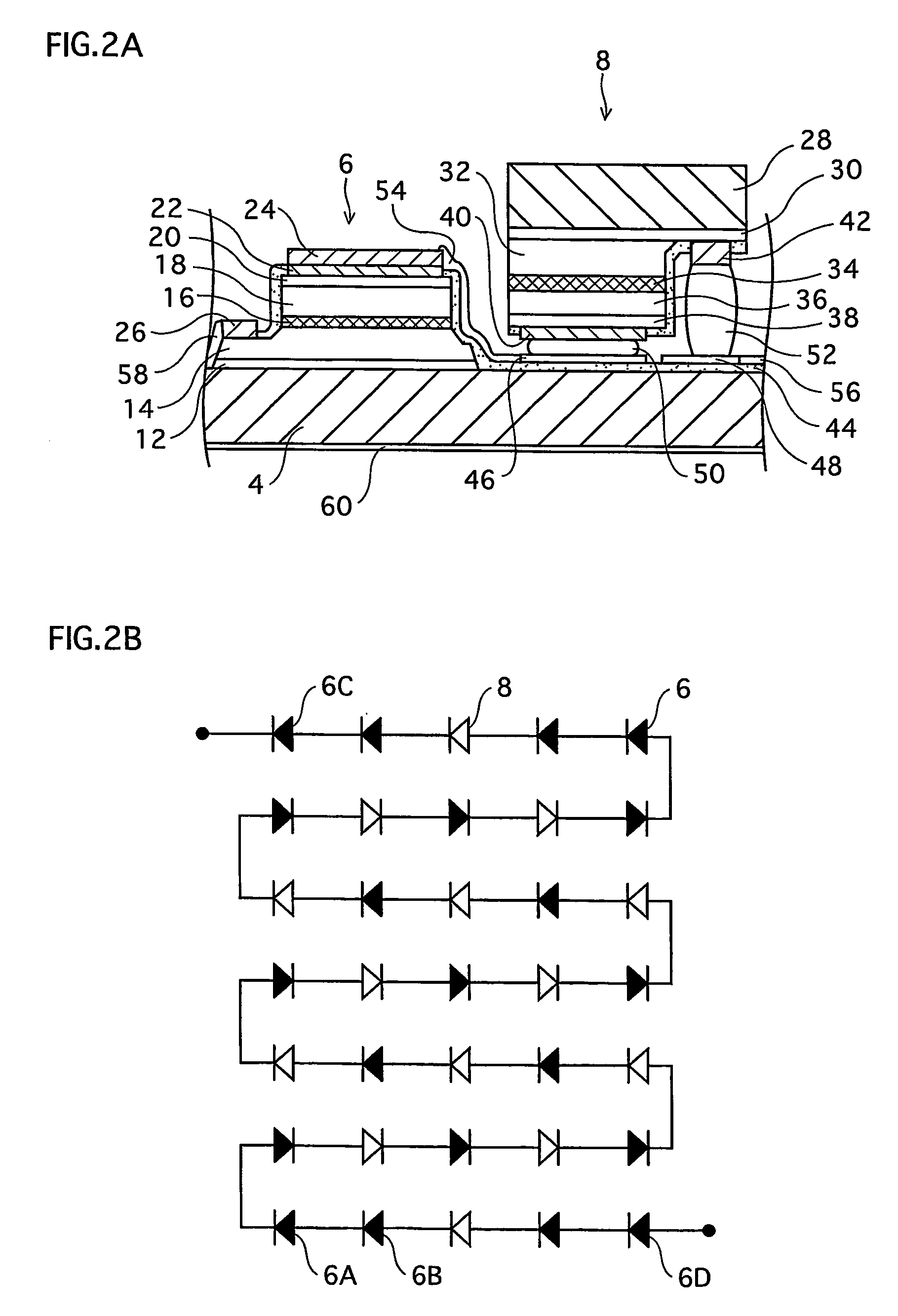
[0040]FIG. 1A is an external perspective view that illustrates a construction of an LED array chip 2 which is one type of a semiconductor light emitting device. FIG. 1B is a plan view illustrating the LED array chip 2. FIG. 1A mainly shows how blue LEDs 6 and red LEDs 8 are arranged, and therefore does not show minute depressions and protrusions on surfaces of the blue and red LEDs 6 and 8 in the LED array chip 2. It should be noted that a reduced scale for each constituent is not uniform in any of the drawings including FIGS. 1A and 1B.

[0041] As shown in FIGS. 1A and 1B, the LED array chip 2 is formed in such a manner that light emitting elements (LEDs 6 and 8) are arranged in a matrix of N rows and M columns (in the present embodiment, a matrix of seven rows and five columns, in total, 35 LEDs) on a non-doped (highly resistive) SiC substrate 4 which is a semiconductor su...


PUM


Abstract

An LED array chip (2) includes blue LEDs (6) and red LEDs (8). The blue LEDs (6) are formed by epitaxial growth on an SiC substrate (4). Bonding pads (46 and 48) are formed on the SiC substrate (4) in a wafer fabrication process. The red LEDs (8) are separately manufactured from the blue LEDs (6), and flip-chip mounted on the bonding pads (46 and 48) formed on the SiC substrate.

Description

TECHNICAL FIELD [0001] The present invention relates to a semiconductor light emitting device, a light emitting module, and a lighting apparatus. The present invention particularly relates to a semiconductor light emitting device that combines light emitting members which emit light of different colors to emit light of a desired color by mixture of the colors of the light, and to a light emitting module and a lighting apparatus including this semiconductor light emitting device. BACKGROUND ART [0002] In the field of light emitting diodes (LEDs) which are one type of semiconductor light emitting devices, vigorous researches have recently been conducted to use white LEDs for lighting, as white LEDs with higher luminance have been developed. Having a feature of point light sources, LEDs are particularly expected to replace halogen lamps and the like that are conventionally used as spotlighting at shops, museums, and showrooms. [0003] A white LED that is widely used at present includes ...

Claims


Application Information

Patent Timeline
IPC IPC(8): H01L33/00H01L33/06F21S2/00F21S8/04F21Y101/02H01L25/075H01L27/15H01L33/08H01L33/30H01L33/42H01L33/48H01L33/50H01L33/56H01L33/58H01L33/62
CPCF21K9/00H01L25/0753H01L27/156H01L2224/48091H01L2224/48465H01L2924/00014H01L2924/00F21Y2105/10F21Y2105/12F21Y2113/13F21Y2115/10
Inventor NAGAI, HIDEOMUKAI, KENJI
Owner PANASONIC CORP
Why Eureka
Try Eureka