Apparatus and method of fabricating emitter using arc

Inactive Publication Date: 2006-08-17
SAMSUNG ELECTRONICS CO LTD
View PDF8 Cites 0 Cited by
  • Summary
  • Abstract
  • Description
  • Claims
  • Application Information

AI Technical Summary

Benefits of technology

[0007] The present invention may provide a simplified method of fabricating an emitter havin

Problems solved by technology

Consequently, the manufacturing time and cost of metal emitters and electric/electronic devices using the metal emitters are increas

Method used


Image

  • Apparatus and method of fabricating emitter using arc
  • Apparatus and method of fabricating emitter using arc
  • Apparatus and method of fabricating emitter using arc

Examples


Example

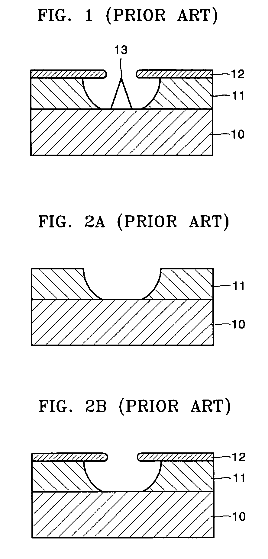
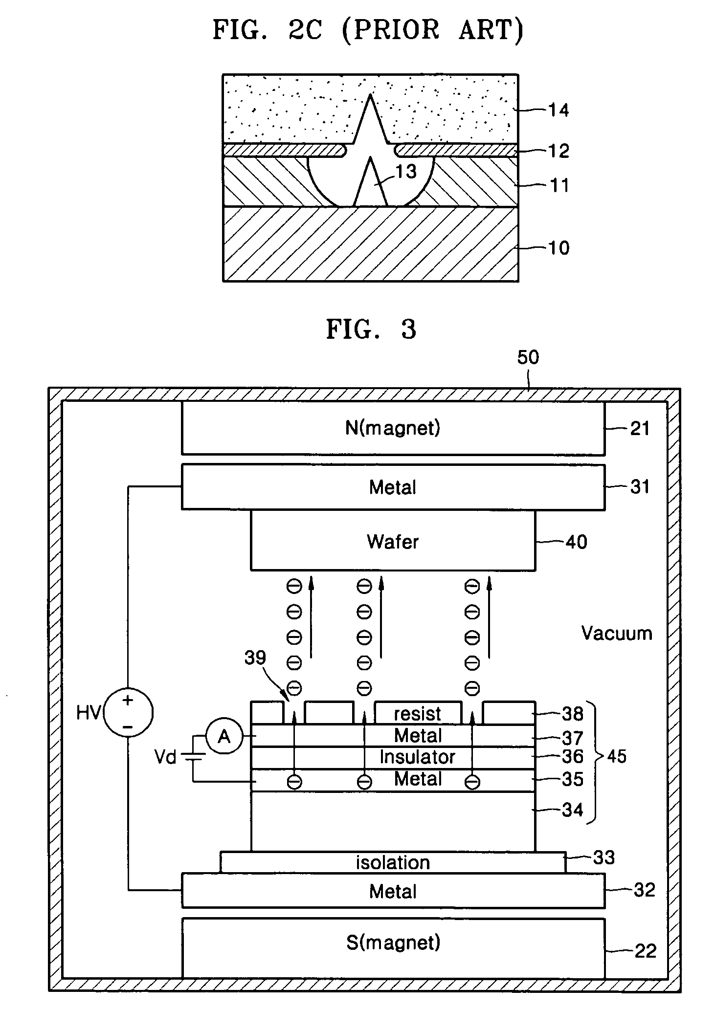
[0028] As described previously, a conventional emitter is formed by a complex semiconductor fabrication method. However, in the present invention, an emitter having a sharp tip is formed on the surface of a wafer by producing a strong arc and instantaneously melting the surface of the wafer.

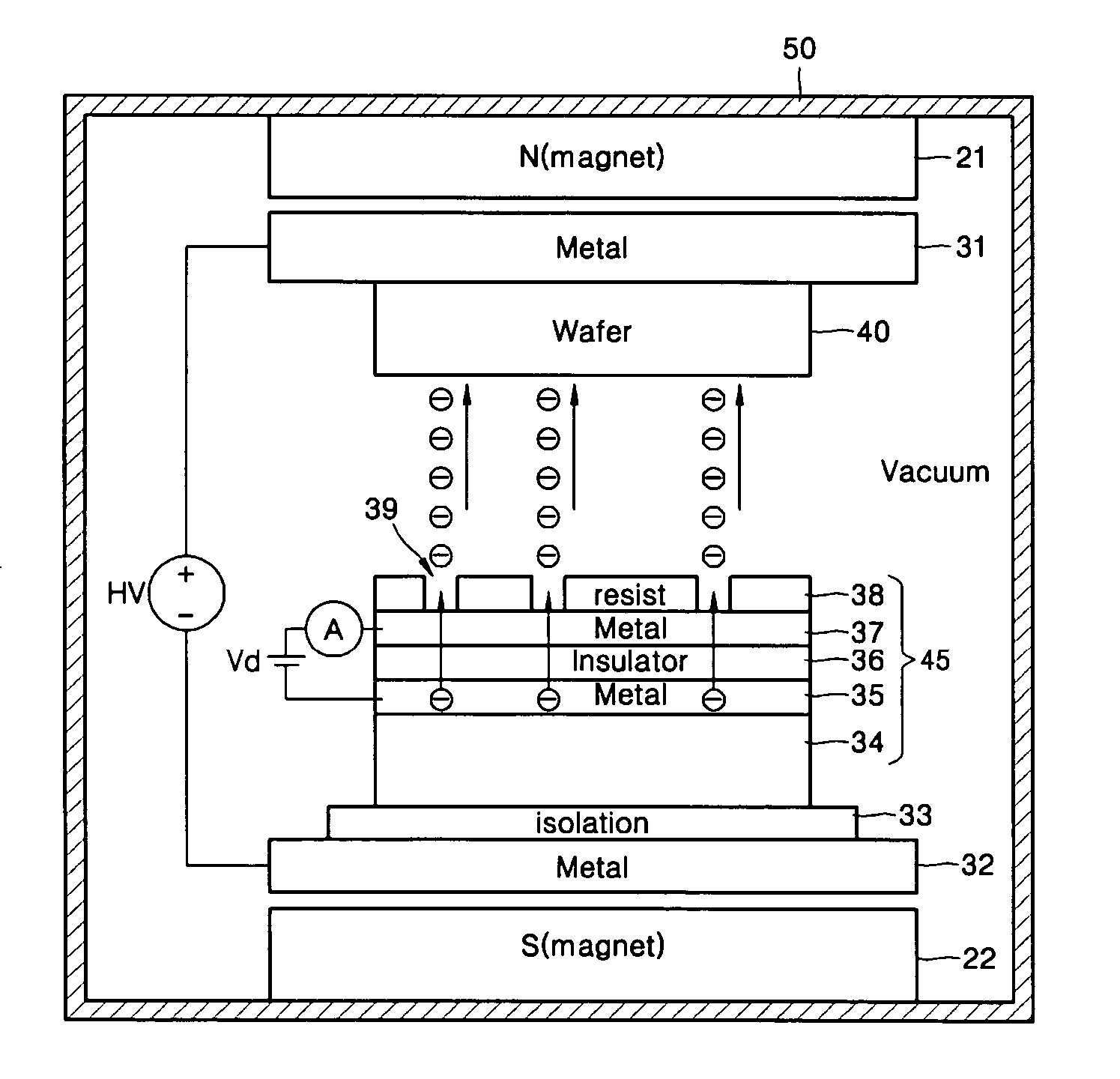
[0029]FIG. 3 is a cross section of an apparatus for fabricating such an emitter using an arc according to an embodiment of the present invention. Referring to FIG. 3, in the apparatus, a device for producing an arc is installed inside a vacuum chamber 50, in which a vacuum is maintained.

[0030] In more detail, a first magnetic pole 21 on a ceiling of the vacuum chamber 50 and a second magnetic pole 22 on a floor of the vacuum chamber 50 are disposed to face each other. The first and second magnetic poles 21 and 22 may be a single bent magnet. It is also possible to install two separate magnets with different polarities in the vacuum chamber 50 to face each other. In the present embodiment, for e...


PUM


Abstract

A method and apparatus for fabricating an emitter by colliding an arc with the surface of a wafer inside a vacuum chamber are provided. The apparatus includes: a vacuum chamber in which a wafer is inserted; a magnetic field generating unit for generating a uniform magnetic field inside the vacuum chamber; an electric field generating unit for forming an electric field parallel to the magnetic field inside the vacuum chamber; and a master emitter for emitting electrons towards the wafer. The electrons emitted from the master emitter move along the magnetic field and the electric field. The arc is generated when the electric field or the driving voltage surpasses a threshold by controlling the strength of the electric field and the driving voltage of the master emitter. Thus, the surface of the wafer is instantaneously melted and solidified by the arc, thereby forming the emitter with a sharp tip on the surface of the wafer.

Description

[0001] This application claims the priority of Korean Patent Application No. 10-2005-0013139, filed on Feb. 17, 2005 in the Korean Intellectual Property Office, the disclosure of which is incorporated herein in its entirety by reference. BACKGROUND OF THE DISCLOSURE 1. Field of the Disclosure [0002] The disclosure relates to an apparatus and method of fabricating an emitter using an arc, and more particularly, to an apparatus and method of fabricating an emitter, which is formed by colliding an arc with the surface of a wafer inside a vacuum chamber. [0003] 2. Description of the Related Art [0004] A next generation display device, for example, a field emission device (FED) uses a metal emitter having an extremely sharp tip of a nano-size. FIG. 1 is an exemplary view of a conventional FED using a metal emitter 13 of this type. As illustrated in FIG. 1, an insulating layer 11 having an opening is formed in a substrate 10 in the FED. A gate 12 is formed on top of the insulating layer 1...

Claims


Application Information

Patent Timeline
IPC IPC(8): H01L21/00H01J7/24
CPCH01J9/025B60Q9/00B60R16/0231B60Y2200/11B60Y2400/30
Inventor MOON, CHANG-WOOKYOO, IN-KYEONG
Owner SAMSUNG ELECTRONICS CO LTD
Why Eureka
Try Eureka