

Liquid crystal panel and fabricating method thereof
- Summary
- Abstract
- Description
- Claims
- Application Information
AI Technical Summary
Benefits of technology
Problems solved by technology
Method used
Image

Examples
first embodiment
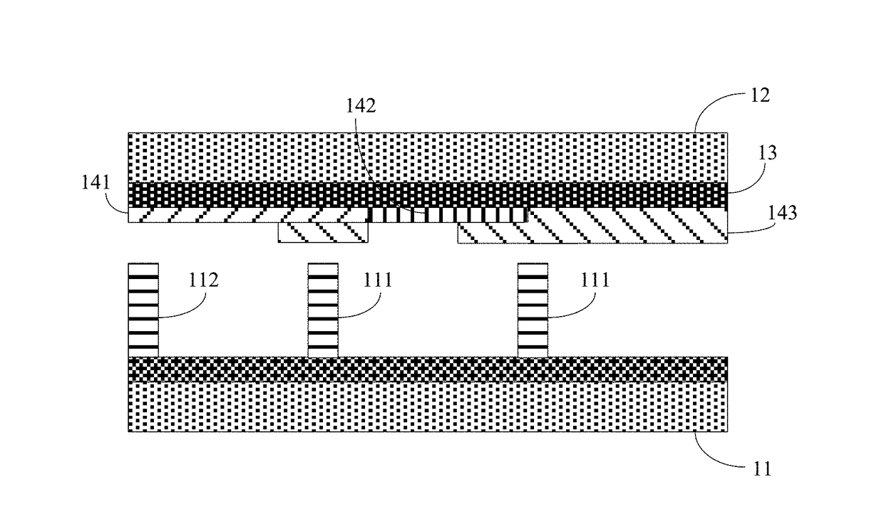
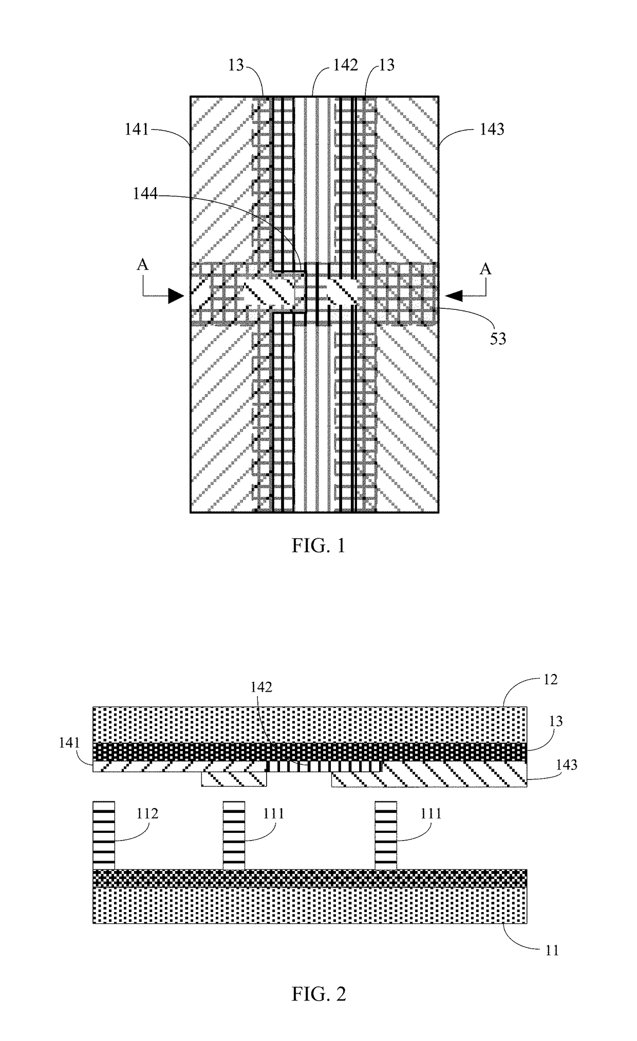
[0033]With reference to FIG. 1 and FIG. 2, FIG. 1 is a structural schematic view of a color film substrate of a liquid crystal of the present invention. FIG. 2 is a cross sectional schematic view taken along A-A line of FIG. 1.
[0034]The liquid crystal panel of the present invention has an array substrate 11, a color film substrate 12 and a liquid crystal layer (not shown in the drawing) mounted between the array substrate 11 and the color film substrate 12.
[0035]The color film substrate 12 has multiple color resists formed thereon and the color resists are formed to multiple color filter units. Particularly, the liquid crystal panel of the present embodiment is an RGB display mode. The color resists of the color film substrate 12 includes a red color resist 141, a green color resist 142 and a blue color resist 143. The red color resist 141 is formed to a red filter unit, the green color resist 142 is formed to a green filter unit and the blue color resist 143 is formed to a blue fil...
second embodiment
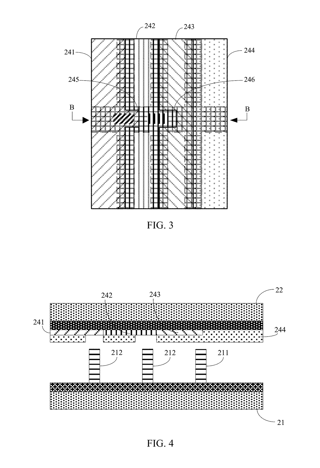
[0050]With reference to FIG. 3 and FIG. 4, FIG. 3 is structural schematic view of the color film substrate of the liquid crystal panel of the present invention. FIG. 4 is a cross sectional schematic view taken along B-B line of FIG. 3.
[0051]A difference between the present embodiment and the first embodiment is that the liquid crystal panel of the present embodiment is an RGBW display module. The color film substrate 22 has four different color resists formed thereon and including the red color resist 241, the green color resist 242, the blue color resist 243 and the white color resist 244. The red, green and blue color resists 241, 242, 243 have the same thickness and the white color resist 244 is thicker than the red color resist 241. For example, the white color resist 244 is 0.3 μm or 0.5 μm thicker than the red color resist 241. It should be noted that the white color resist 244 of the present invention may be used as a flat layer to provide the color film substrate 22 a flat f...
third embodiment
[0059]With reference to FIG. 5 and FIG. 6, FIG. 5 is a structural schematic view of the color film substrate of the liquid crystal panel of the present invention. FIG. 6 is a cross sectional schematic view taken along C-C line of FIG. 5.
[0060]The liquid crystal panel of the present embodiment is an RGB display mode, the color film substrate 32 of the liquid crystal panel has the red, green and blue color resists 341, 342, 343 formed thereon. The red and green color resists 341, 342 have the same thickness, and the blue color resist 343 is thicker than the red color resist 341.
[0061]The array substrate 31 has the first, second and third spacers 311, 312, 313 formed thereon. Further, the first and second spacers 311 and 312 have the same height. The blue color resist 343 corresponding to the first spacer 311 is thicker than the red color resist 341 corresponding to the second spacer 312.
[0062]The third spacer 313 is higher than the second spacer 312. The color resist corresponding to ...
PUM
 Abstract
Description
Claims
Application Information