
Double-sided electrodynamic screen films

Active Publication Date: 2020-02-27
EASTMAN KODAK CO
View PDF17 Cites 1 Cited by
  • Summary
  • Abstract
  • Description
  • Claims
  • Application Information

AI Technical Summary

Benefits of technology

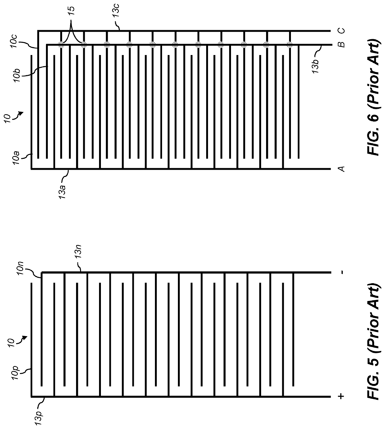
The invention allows for electrode patterns on a transparent film to be placed on the same side without overlapping, which eliminates the need for insulating layers and reduces cost. It also improves reliability by preventing shorts caused by breakdown of insulating materials at cross-over points.

Problems solved by technology

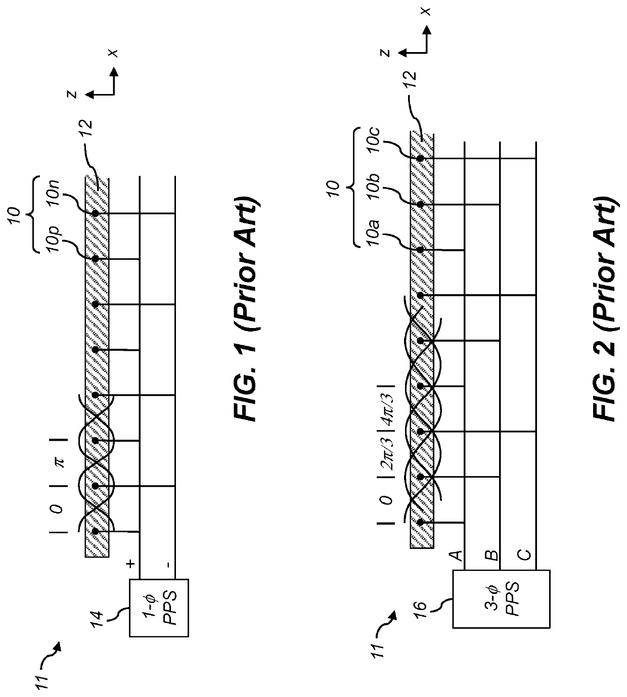
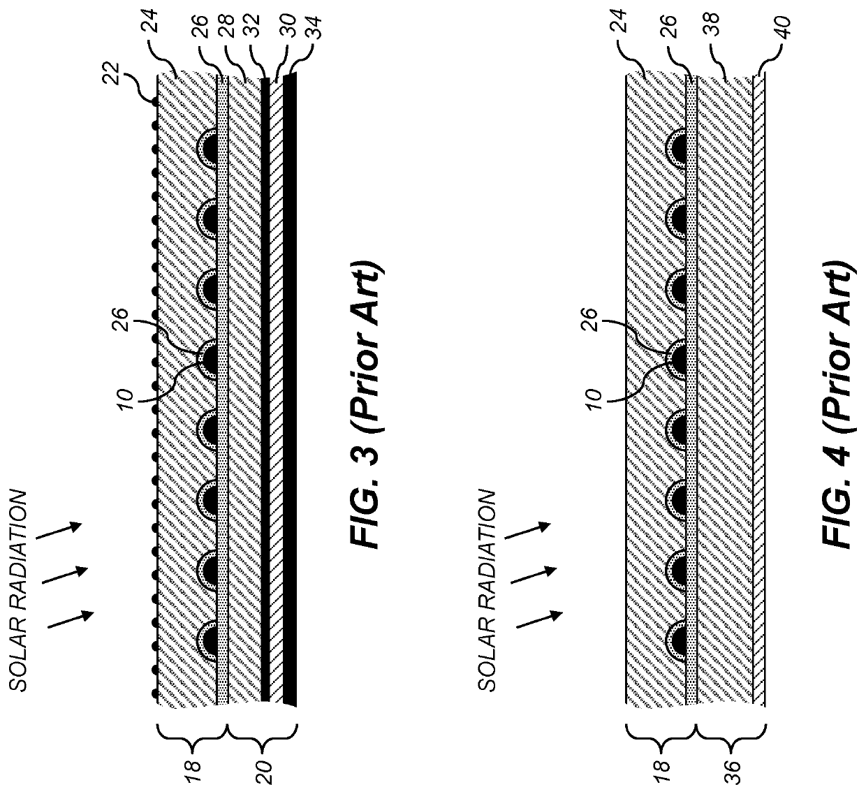
Some of the major difficulties in applying EDS on solar panels include: (1) avoiding interactions between the electric field of the EDS electrodes and current collecting grids used in solar panels for providing electrical power; (2) scaling of the method of EDS construction for manufacturing and installing transparent electrodes on solar panels and solar concentrators; (3) obscuration of solar radiation caused by the placement of the EDS on the surface of solar panels and concentrators; (4) retrofitting existing solar photovoltaic and photothermal devices with self-cleaning EDS systems; (5) environmental degradation of polymer films under outdoors condition; (6) maintaining the efficiency of heat dissipation of solar panels integrated with EDS; and (7) cost-effective manufacturing of new solar panels and solar concentrators integrated with EDS for large-scale installations.
This patterned dielectric adds manufacturing complexity due to additional process and pattern-alignment steps.
Additionally, the patterned dielectric materials typically suffer from robustness issues, with defects or inherent materials properties leading to dielectric breakdown and electrode shorting.
However, the current-carrying capacity of such electrodes is limited, thereby limiting the length of electrode due to the resultant resistive losses.
Moreover, the substrate materials are limited by the electrode material deposition process (e.g., sputtering).
Thicker layers of metal oxides or metals can increase conductivity but reduce the transparency of the electrodes.
However, such wires are not transparent and thus the number and size of the wires limits the substrate transparency as the overall conductivity of the wires increases.
There is a conflict between the optical transparency and the conductivity (or surface resistance) of transparent electrodes.

Method used


Image

  • Double-sided electrodynamic screen films
  • Double-sided electrodynamic screen films
  • Double-sided electrodynamic screen films

Examples


Embodiment Construction

[0042]The present description will be directed in particular to elements forming part of, or cooperating more directly with, an apparatus in accordance with the present invention. It is to be understood that elements not specifically shown, labeled, or described can take various forms well known to those skilled in the art. It is to be understood that elements and components can be referred to in singular or plural form, as appropriate, without limiting the scope of the invention.

[0043]The invention is inclusive of combinations of the embodiments described herein. References to “a particular embodiment” and the like refer to features that are present in at least one embodiment of the invention. Separate references to “an embodiment” or “particular embodiments” or the like do not necessarily refer to the same embodiment or embodiments; however, such embodiments are not mutually exclusive, unless so indicated or as are readily apparent to one of skill in the art. It should be noted th...


PUM


Abstract

An electrode film includes a first electrode pattern having a first set of parallel conductive electrodes and a second electrode pattern having a second set of parallel conductive electrodes disposed on a first surface of a transparent film, wherein elements of the first electrode pattern do not cross over elements of the second electrode pattern. A third electrode pattern having a third set of parallel conductive electrodes is disposed on a second surface of the transparent film, wherein the first, second and third sets of parallel conductive electrodes are arranged in an interlaced pattern. The electrode patterns are configured to be connected to respective power sources of electrical power supplying respective waveforms to generate a time-varying electric field pattern above a surface of the electrode film.

Description

CROSS-REFERENCE TO RELATED APPLICATIONS[0001]Reference is made to commonly assigned, co-pending U.S. patent application Ser. No. ______ (Docket K002243), entitled: “Open electrodes for in-plane field generation,” by C. Liston et al.; and to commonly assigned, co-pending U.S. patent application Ser. No. ______ (Docket K002261), entitled: “Fabricating double-sided electrodynamic screen films,” by D. Garman et al., each of which is incorporated herein by reference.STATEMENT REGARDING FEDERALLY-SPONSORED RESEARCH OR DEVELOPMENT[0002]This invention was made with Government support under # DE-EE0007119 awarded by DOE. The Government has certain rights in this invention.FIELD OF THE INVENTION[0003]This invention pertains to the field of electrodynamic screen films, and more particularly to a novel electrode configuration.BACKGROUND OF THE INVENTION[0004]In-plane electric fields are used for the alignment of liquid crystals and other molecules, or for the movement of charged particles. In-p...

Claims


Application Information

Patent Timeline
IPC IPC(8): B08B6/00H02S40/10A47L1/02F24S40/20
CPCA47L1/02B08B6/00H02S40/10F24S40/20Y02B10/20Y02E10/40Y02E10/50
Inventor TOMBS, THOMAS NATHANIELSPATH, TODD MATHEWGARMAN, DOUGLAS EDWARDELLINGER, CAROLVN RAELISTON, CHRISTOPHER B.
Owner EASTMAN KODAK CO
Learn More