Image sensor having improved sensitivity and method for making same

a technology of image sensor and sensitivity, which is applied in the direction of radio frequency controlled devices, semiconductor devices, electrical apparatus, etc., can solve the problems of affecting the electrical characteristics of underlying transistors or other elements, requiring higher power consumption and lower speed operation than the cis type, and generally difficult to form aluminum interconnections for semiconductor devices, etc., to achieve the effect of higher refractive index

Inactive Publication Date: 2006-08-17
SAMSUNG ELECTRONICS CO LTD
View PDF6 Cites 112 Cited by
  • Summary
  • Abstract
  • Description
  • Claims
  • Application Information

AI Technical Summary

Benefits of technology

[0011] According to an alternative embodiment of the invention, the fifth interlayer dielectric may be about 1.5 to about 3 times thicker than its adjacent layers of interlayer dielectrics. The interlayer dielectrics may be made of transparent material. The filling material may have a higher refractive index than the interlayer dielectrics, and may be made from a resin or flowable oxide, and may contact the photo conversion elements. The first flattening layer may be about 0.2 μm to about 0.6 μm in thickness. The interlayer dielectrics may have substantially the same thickness except for the first interlayer dielectric. The interconnections may be made of copper. The substrate may be made of silicon or SOI. The method may further include another flattening layer between the filling material and the color filters.

Problems solved by technology

CCD sensors operate with low noise and device uniformity, but generally require higher power consumption and lower speed operation than the CIS type.
Aluminum has traditionally been used in the integrated circuit (IC) industry as a metal for making electrical interconnections in IC devices; however, it is generally difficult to form aluminum interconnections for a semiconductor device having a design rule or pattern thickness below 0.13 μm.
However, copper atoms tend to diffuse into surrounding materials, such as into an interlayer dielectric layer, and can negatively impact the electrical characteristics of underlying transistors or other elements.
However, these materials are opaque, and would block the passage of the optical signals unless they are removed from the optical passages 88.
Although the gap filling material must, of course, be optically transparent, a significantly thick amount of the gap filing material would nevertheless impede and reduce the level of optical signals from reaching the photo conversion elements 52.

Method used


Image

  • Image sensor having improved sensitivity and method for making same
  • Image sensor having improved sensitivity and method for making same
  • Image sensor having improved sensitivity and method for making same

Examples


Embodiment Construction

[0027] The present invention will now be described more fully hereinafter with reference to the accompanying drawings, in which preferred embodiments of the invention are shown. In the drawings, the thickness of layers and regions are exaggerated for clarity. Like numbers refer to like elements throughout.

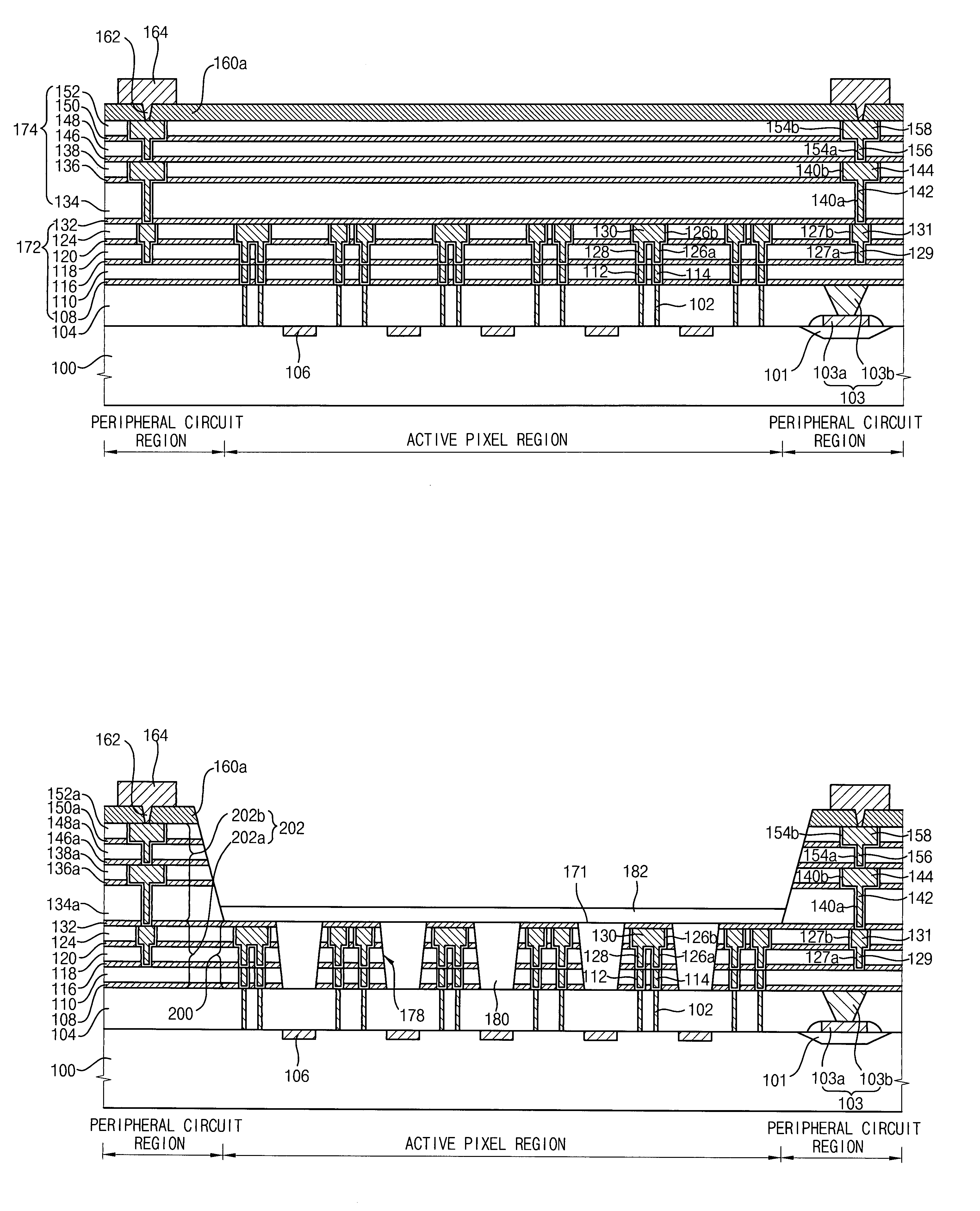
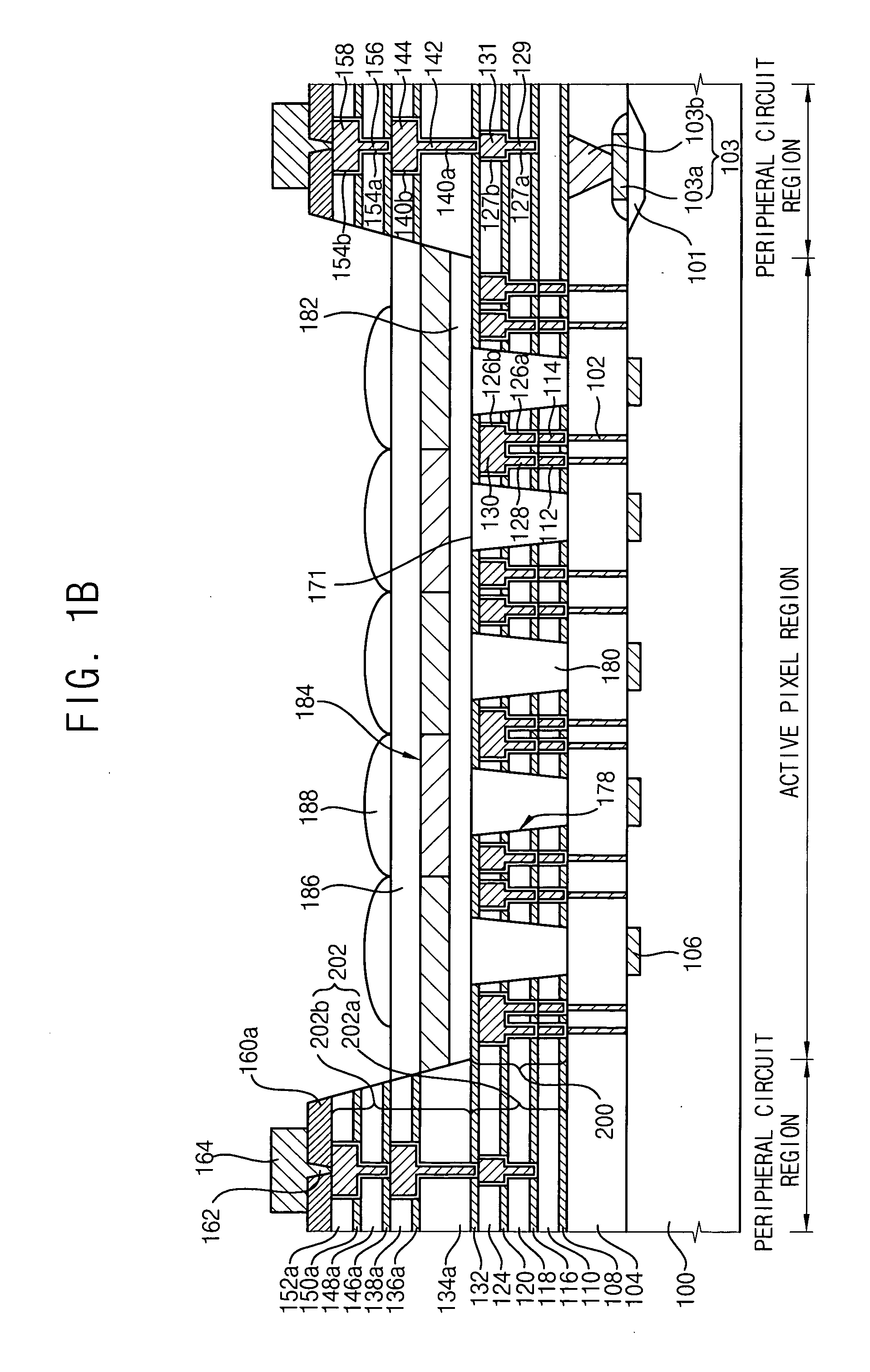
[0028] In an embodiment of the present invention, an image sensor device is provided as illustrated in FIG. 1 B. The image sensor device is preferably of the CIS type, divided into an active pixel region and peripheral circuit regions over a common substrate 100. Photo conversion elements and associated interconnections, color filters, and lens assembly are disposed in the active pixel region. Peripheral interconnections, contacts, isolation region, and circuit pads are formed in the peripheral circuit region.

[0029] The photo conversion elements 106 are formed in the active pixel region of the substrate 101. A first interlayer dielectric 104 is formed above the substrate 100. Fir...


PUM


Abstract

An image sensor having improved sensitivity and method for making same include a substrate having an active pixel region with a peripheral circuit region surrounding the active pixel region; a plurality of photo conversion elements disposed in the active pixel region, each photodiode is configured for receiving light through a lens and an opening formed between a plurality of layers of interlayer dielectrics formed on top of each other above the substrate; and a plurality of interconnections electrically connecting to the photo conversion elements disposed within the active pixel region, wherein the distance between the lens and the photo conversion elements is shorter than the distance between the substrate and the top interlayer dielectric in the peripheral circuit region.

Description

BACKGROUND OF THE INVENTION [0001] 1. Technical Field [0002] The present invention relates to a structure of an image sensor device and a method for fabricating the same. More particularly, the present invention relates to an image sensor device having a copper interconnection and improved sensitivity and a method for fabricating the same. [0003] 2. Discussion of the Related Art [0004] Semiconductor image sensing devices are widely used for capturing images in a variety of applications such as digital cameras, camcorders, printers, scanners, etc. The semiconductor image sensing devices include image sensors that capture optical information and convert the optical information into electrical signals, which are then processed, stored, and otherwise manipulated to result in projection of the captured images onto a display or print medium. There are two types of image sensor devices which are widely used: a charge coupled device (CCD) type and CMOS image sensors (CISs) type. CCD sensors...

Claims


Application Information

Patent Timeline
Patent Type & Authority Applications(United States)
IPC IPC(8): H01L21/00
CPCH01L27/14627H01L27/14632H01L27/14636H01L27/14687H01L27/146
Inventor OH, TAE SEOKYI, DUK MINLEE, JUNE TAEG
Owner SAMSUNG ELECTRONICS CO LTD
Why Eureka
Try Eureka