Ultrasonic element

a technology of ultrasonic element and ultrasonic sensing device, which is applied in the direction of mechanical vibration separation, piezoelectric/electrostrictive/magnetostrictive device, piezoelectric/electrostrictive/magnetostriction machine, etc. it can solve the problems of increasing product cost, practically impossible to detect obstacles, and emitting purpose, so as to reduce the manufacturing cost of ultrasonic sensing device, reduce the stiffness of the membrane at such stress

Inactive Publication Date: 2006-08-24
DENSO CORP
View PDF12 Cites 51 Cited by
  • Summary
  • Abstract
  • Description
  • Claims
  • Application Information

AI Technical Summary

Benefits of technology

[0017] According to a further feature of the present invention, an ultrasound receiving element can be formed in the same substrate together with but at a different position from the ultrasound emitting element. Accordingly, the manufacturing cost of the ultrasonic sensing device can be made lower and it becomes easier to install the ultrasonic sensing device in the automotive vehicle, when compared with the case in which the emitting element a

Problems solved by technology

On the other hand, the MEMS type ultrasonic element 90 shown in FIGS. 10A and 10B is an ultrasonic element for an exclusive use of receiving, and consequently unusable at present for emitting purpose due to difficulty in outputting ultrasonic waves of sufficient sound pressure.
Therefore, it is practically impossible to detect an obstacle,

Method used


Image

  • Ultrasonic element
  • Ultrasonic element
  • Ultrasonic element

Examples


first embodiment

(First Embodiment)

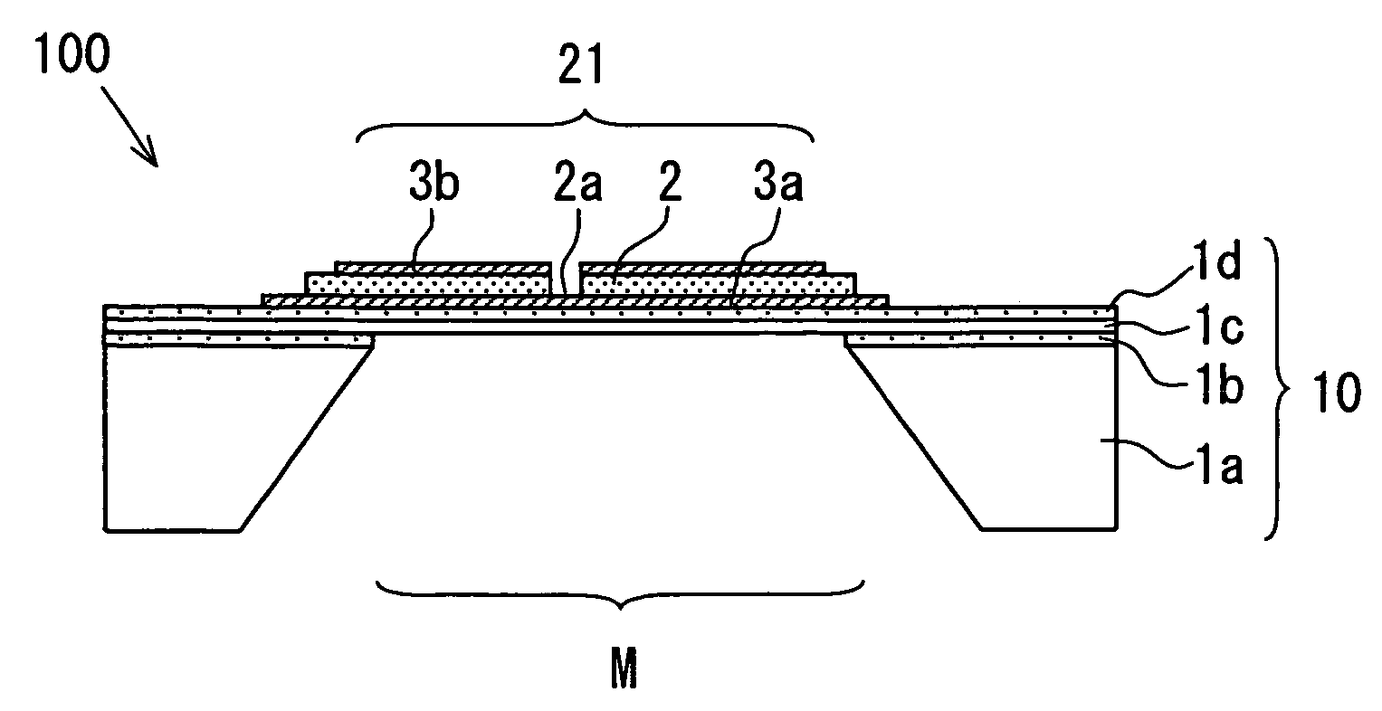
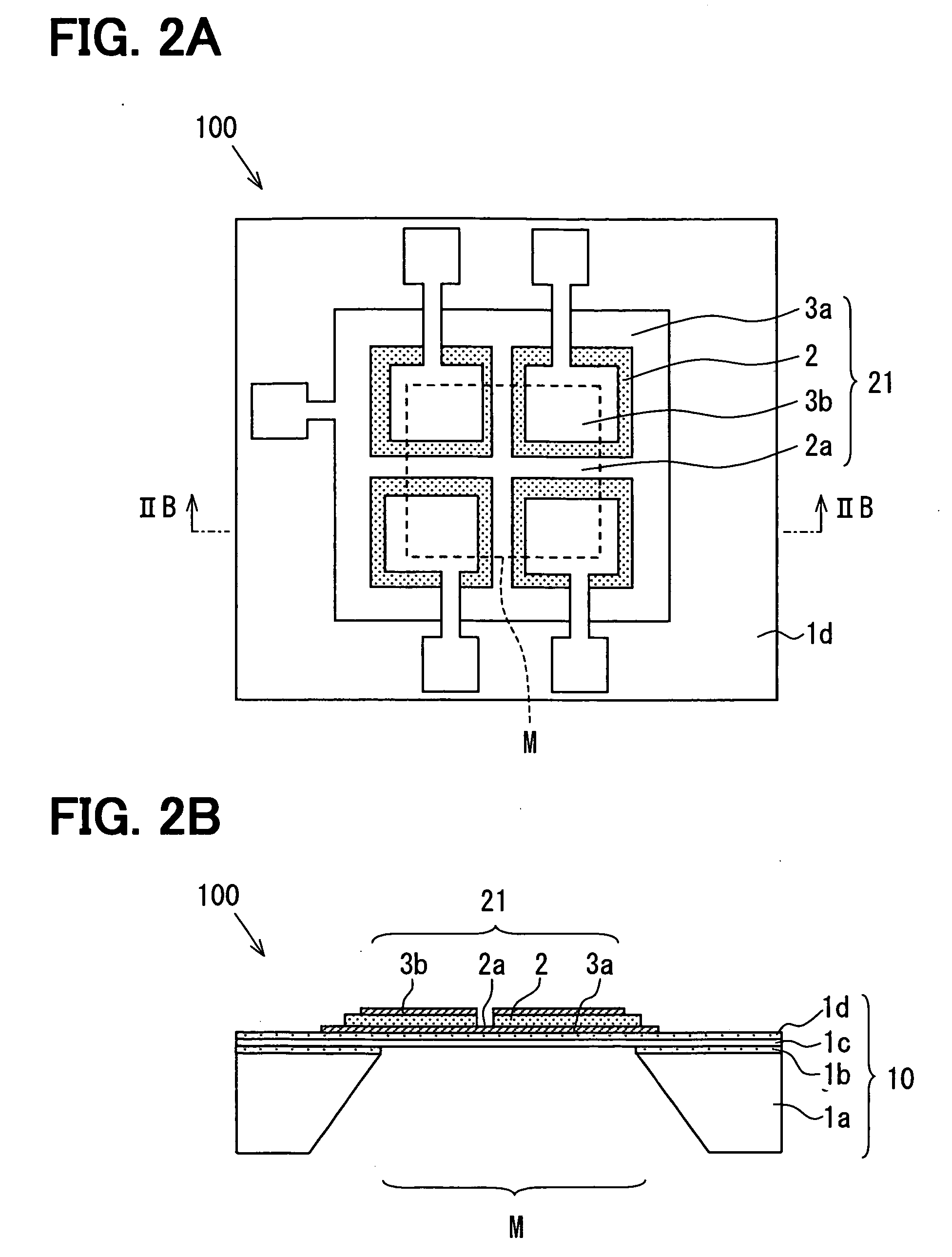
[0051]FIG. 2A is a schematic top plan view of the ultrasonic element 100 of the embodiment of the present invention, and FIG. 2B is a cross sectional view taken along a line IIB-IIB indicated by a one-dot-chain line in FIG. 2A.

[0052] The ultrasonic element 100 shown in FIGS. 2A and 2B is manufactured by using the semiconductor substrate 10 having the structure of SOI (Silicon On Insulator). Namely, a piezoelectric vibrator 21 is formed on a membrane M so as to wholly cover the membrane M, which is formed as a thin film portion (a thin walled portion) of the substrate 10, wherein the substrate 10 of the SOI structure comprises a first semiconductor layer (a supporting substrate) 1a, a buried oxide film 1b, a second semiconductor layer 1c, and a protection oxide film 1d. A plane shape of the membrane M is of a square form, and such square shaped membrane M can be easily processed and manufactured by the semiconductor micromachining technology. The ultrasonic element...

second embodiment

(Second Embodiment)

[0075] According to the second embodiment, shallow groove patterns are partially formed in the piezoelectric thin film in the vicinity of the stress concentrated areas, in order that the stiffness of the membranes in the vicinity of the stress concentrated areas is decreased to thereby make the membranes easily deform.

[0076]FIG. 6A is a schematic top plan view of an ultrasonic element 110 of this embodiment, whereas FIG. 6B is a cross sectional view taken along a line VIB-VIB indicated by a one-dot-chain line in FIG. 6A. In the ultrasonic element 110 in FIGS. 6A and 6B, the same reference numerals are used to designate the same portions as the ultrasonic element 100 of FIGS. 2A and 2B.

[0077] The ultrasonic element 110 shown in FIGS. 6A and 6B, is likewise manufactured by the semiconductor substrate 10 having the SOI structure, as in the same manner to the ultrasonic element 100 shown in FIGS. 2A and 2B.

[0078] In the piezoelectric vibrator 21 of the ultrasonic e...

third embodiment

(Third Embodiment)

[0081] The third embodiment relates to an ultrasonic element having a multi-layered piezoelectric vibrator.

[0082]FIG. 7A is a schematic top plan view of the ultrasonic element 120 of this embodiment, FIG. 7B is a cross sectional view taken along a line VIIB-VIIB indicated by a one-dot-chain line in FIG. 7A, and FIG. 7C is an enlarged view of a portion of the multi-layered piezoelectric vibrator. In the ultrasonic element 120 in FIGS. 7A to 7C, the same reference numerals are used to designate the same portions as the ultrasonic element 90 of FIGS. 10A and 10B.

[0083] The ultrasonic sensing element 120 shown in FIGS. 7A to 7C, is likewise manufactured by the semiconductor substrate 10 having the SOI structure, as in the same manner to the ultrasonic element 90 shown in FIGS. 10A and 10B.

[0084] The piezoelectric vibrator 20 of the ultrasonic element 90 of FIGS. 10A and 10B has one layer of the piezoelectric thin film 2, whereas the piezoelectric vibrator 29 of the ...


PUM


Abstract

An ultrasonic element has a membrane formed as a thin walled portion of a substrate, on which a piezoelectric vibrator is formed. The piezoelectric vibrator comprises a piezoelectric thin film and metal electrode films, which are formed into a sandwiched structure. The piezoelectric vibrator resonates with the membrane at a predetermined ultrasonic wave-band frequency. A hollow-out pattern is formed in the piezoelectric thin film to divide the piezoelectric vibrator into multiple portions, wherein the hollow-out pattern is formed in such an area corresponding to stress concentrated area which appears in vibrations of the membrane in diametrical directions thereof. The membrane is made to be easily deformed in response to vibration of the piezoelectric vibrator, so that an ultrasound of a higher sound pressure can be emitted.

Description

CROSS-REFERENCE TO RELATED APPLICATION [0001] This application is based on Japanese Patent Application No. 2005-044805 filed on Feb. 21, 2005, disclosure of which is incorporated herein by reference. FIELD OF THE INVENTION [0002] The present invention relates to an ultrasonic element (or an ultrasonic wave element) having a piezoelectric vibrator formed on a membrane (or a diaphragm) and being capable of resonance with the membrane at a prescribed ultrasonic wave-band frequency, and more particularly relates to an ultrasonic element usable for obstacle detection and / or other purposes in the field of automotive vehicles. BACKGROUND OF THE INVENTION [0003] An ultrasonic sensing equipment, which is mounted on a vehicle, such as an automobile, and used for detecting a distance between the vehicle and surrounding obstacles at the time of parking or turning thereof, is disclosed, for example, in Japanese Patent Publication No. 2001-16694. Such an ultrasonic sensing equipment is comprised ...

Claims


Application Information

Patent Timeline
IPC IPC(8): H01L41/08
CPCB06B1/0692H03H3/02H03H9/02133H03H9/172H03H9/564H03H9/583H03H9/588
Inventor SUGIURA, MAKIKOITOH, TOMOKI
Owner DENSO CORP
Why Eureka
Try Eureka