Solid-state imager device, drive method of solid-state imager device and camera apparatus

a solid-state imager and drive method technology, applied in the direction of color signal processing circuits, television systems, radio control devices, etc., can solve the problems of non-uniform scanning lines in imaged pictures, collapse of spectral diffraction balance, etc., to inhibit reduce the thickness of insulation films, and reduce the generation of leakage current

Active Publication Date: 2006-08-24
SONY CORP
View PDF11 Cites 83 Cited by
  • Summary
  • Abstract
  • Description
  • Claims
  • Application Information

AI Technical Summary

Benefits of technology

[0023] In a solid-state imager device and a camera apparatus of the present invention, generation of a dark current from the boundary surface of the substrate rear surface side decreases by applying a voltage of reverse-polarity with respect to the potential of the semiconductor substrate to the rear surface electrode as mentioned above. Further, there can be provided with a leakage current inhibiting region just under the pad portion, so that even if a needle for inspection is to be applied to the pad portion many times, insulation film destruction under the rear surface electrode can be prevented or even if the insulation film is destroyed, it is possible to inhibit the leakage current between the pad portion and the semiconductor substrate.
[0024] According to a solid-state imager device and a camera apparatus relating to the present invention, it is possible to fabricate a structure equivalent to a positive hole accumulation layer (or electron accumulation layer) on the boundary surface of t...

Problems solved by technology

However, the apparatus for laser annealing is expensive and also, it scans wafers sequentially so that the throughput thereof is bad when compared with a diffusion furnace which can handle dozens of wafers all at once and furthermore, it sometimes...

Method used


Image

  • Solid-state imager device, drive method of solid-state imager device and camera apparatus
  • Solid-state imager device, drive method of solid-state imager device and camera apparatus
  • Solid-state imager device, drive method of solid-state imager device and camera apparatus

Examples


first exemplified embodiment

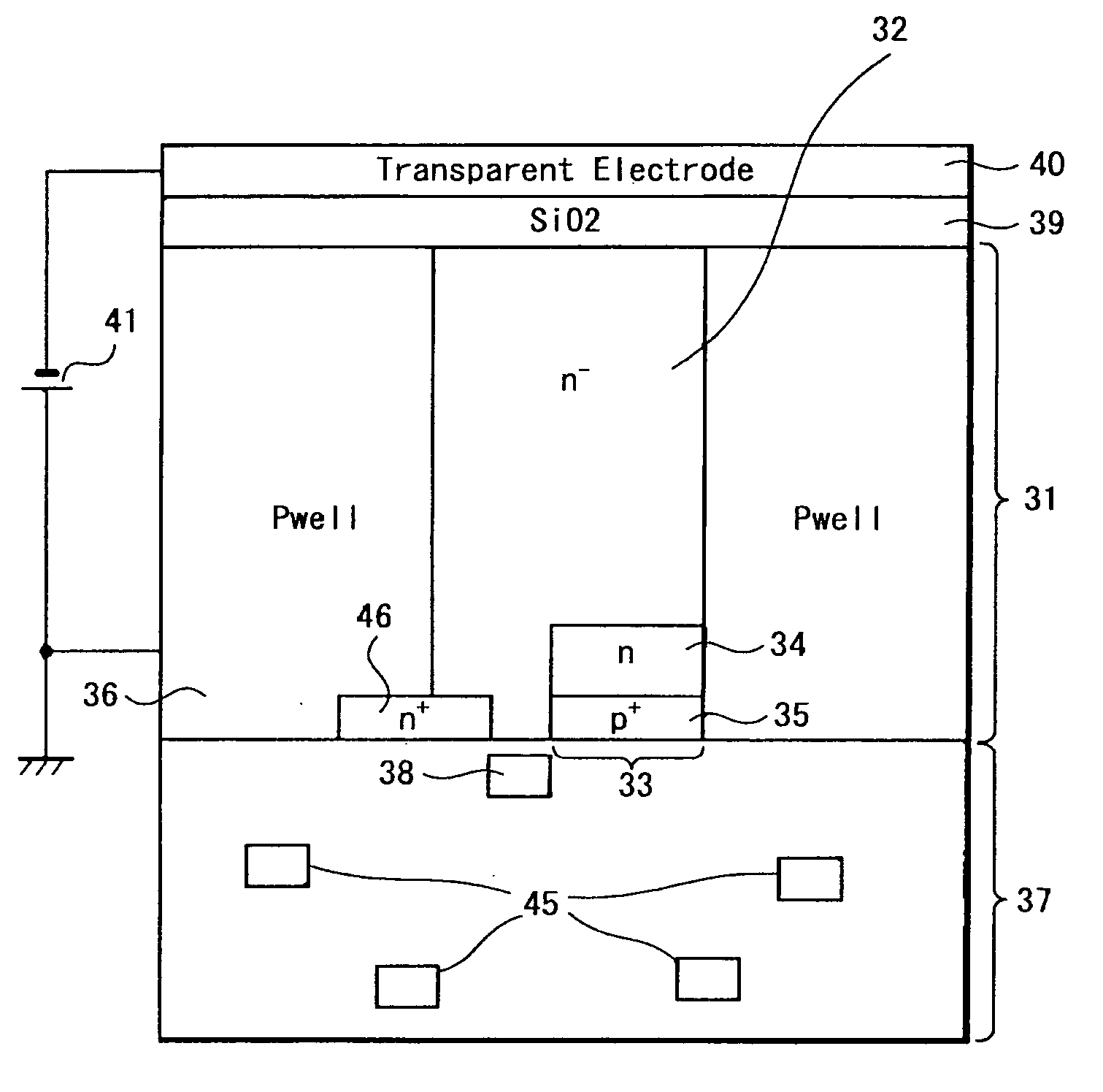
[0063]FIG. 5 is a cross section diagram showing a main portion of a CMOS imager sensor of a rear surface incidence type and more particularly that pixel structure of the rear-surface light receiving type relating to a first exemplified embodiment of the present invention. In the pixel structure of the rear-surface light receiving type relating to this exemplified embodiment, a first conductivity type, for example, n type (n−) silicon substrate is used as the semiconductor substrate.

[0064] In the FIG. 5, by polishing a wafer using CMP (Chemical Mechanical Polishing), a predetermined thickness of a silicon portion (hereinafter, described as “silicon substrate”) 31 is formed and a photodiode 33 (corresponding to photodiode 111 of FIG. 4) is formed in this silicon substrate 31 by utilizing aforesaid substrate (n− type region 32). It is preferable for the thickness of the silicon substrate 31 to be around 5 μm to 10 μm with respect to visible light. According to the thickness setting, i...

second exemplified embodiment

[0085] In the first exemplified embodiment, it was assumed that around −3V voltage is applied to the insulation film 39 by using the transparent electrode 40 and the voltage supply source 41, but in the second exemplified embodiment, a transparent electrode is formed on the insulation film 39 by using a material possessing work function difference which applies substantially a negative voltage with respect to the silicon and it is constituted such that the negative voltage of the work function difference of the transparent electrode and the negative voltage by the voltage supply source 41 are used together and to be applied to the insulation film 39.

[0086] It should be noted that it is not always necessary for the transparent electrode consisting of a material possessing the work function difference which applies a negative voltage to be a transparent electrode beyond all over the whole surface similarly as in a case of the first exemplified embodiment and it is allowed only if it ...

third exemplified embodiment

[0091]FIG. 6 is a cross section diagram showing a main portion of a CMOS imager sensor of a rear surface incidence type, in particular a pixel structure of the rear-surface light receiving type relating to a third exemplified embodiment of the present invention wherein portions corresponding to those in FIG. 5 are shown in the drawing by putting the same reference numerals thereof.

[0092] In the pixel structure of the rear-surface light receiving type relating to the third exemplified embodiment, it is same as the cases of the first and the second exemplified embodiments with respect to an aspect where a structure is employed in which the insulation film 39 is provided on the rear surface of the silicon substrate and at the same time, by applying aforesaid insulation film 39 with a voltage of reverse-polarity with respect to that of the potential of the silicon substrate 31, for example, with a voltage of around −3V, positive holes are accumulated on the silicon boundary surface of ...


PUM


Abstract

In a case when a structure of forming a p+ layer on a substrate rear surface side is employed in order to prevent dark current generation from the silicon boundary surface, various problems occur. According to this invention, an insulation film 39 is provided on a rear surface on a silicon substrate 31 and a transparent electrode 40 is further provided thereon, and by applying a negative voltage with respect to the potential of the silicon substrate 31 from a voltage supply source 41 to the insulation film 39 through the transparent electrode 40, positive holes are accumulated on a silicon boundary surface of the substrate rear surface side and a structure equivalent to a state in which a positive hole accumulation layer exists on aforesaid silicon boundary surface is to be created. Thus, various problems in the related art can be avoided.

Description

CROSS REFERENCES TO RELATED APPLICATIONS [0001] The present invention contains subject manner related to Japanese Patent Application JP 2005-043357 filed in the Japanese Patent Office on Feb. 21, 2005, and Japanese Patent Application JP 2005-366916 filed in the Japanese Patent Office on Dec. 20, 2005, the entire contents of which being incorporated herein by reference. BACKGROUND OF THE INVENTION [0002] 1. Field of the Invention [0003] The present invention relates to a solid-state imager device and a drive method of a solid-state imager device and more particularly relates to a rear surface incidence type solid-state imager device which takes in incident light from the rear surface side of the substrate (from the opposite side of the wiring forming side), a drive method of that solid-state imager device and a camera apparatus thereof. [0004] 2. Description of the Related Art [0005] In a solid-state imager device, for example, in an X-Y address type solid-state imager device represe...

Claims


Application Information

Patent Timeline
IPC IPC(8): H04N5/335H01L27/146H04N5/361H04N5/374H04N5/376
CPCH01L27/14609H01L27/14632H01L27/1464H01L27/14643H01L27/14636F24F13/20F24F1/32F24F1/34
Inventor MABUCHI, KEIJIKARASAWA, NOBUHIRO
Owner SONY CORP
Why Eureka
Try Eureka