
Hub chip for connecting one or more memory chips

Inactive Publication Date: 2006-08-24
INFINEON TECH AG
View PDF10 Cites 29 Cited by
  • Summary
  • Abstract
  • Description
  • Claims
  • Application Information

AI Technical Summary

Benefits of technology

[0010] It is an object of the present invention to provide a hub chip which provides a greater level of reliability during operation in a computer system and provides greater transparency about errors which have occurred.
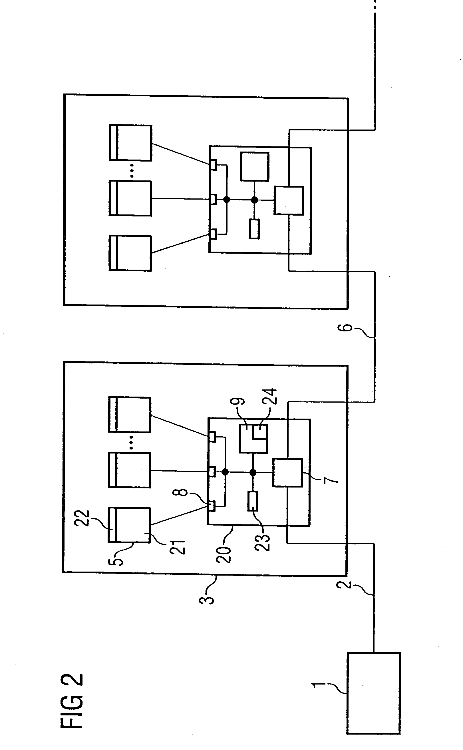
[0012] The inventive hub chip has the advantage that it has an error recognition unit which allows an error which occurs in one of the connected memory chips to be detected. This is done using checking data which are made available to the error recognition unit. The errors recognized can be used to inform the computer system in which the hub chip is preferably being used about the error which has occurred or to repair the error using the checking data. Provision may be made for the hub chip to have a further memory chip interface utilized to receive the checking data, e.g., from a further memory chip, in order to check the contents of the memory areas of the connected memory chips. In this way, the checking data can easily be made available to the hub chip.
[0013] The address decoder unit may be designed to store or read useful data in a first portion of the memory areas of the connected memory areas of the chips and to store or read the checking data in a second portion of the memory areas, said checking data being able to be used to check the contents of the memory areas of the connected memory chips using the error recognition unit. As a result, it is possible to avoid providing the further memory chip interface and the further memory chip connected thereto and instead to cover the additional memory requirement for the checking data using the connected memory chips.
[0015] Provision may also be made for the error recognition unit to have an error correction unit so as to correct erroneous useful data on the basis of the checking data, particularly using a Humming code method. The error correction unit allows for errors which occur in the connected memory chips to be corrected using the additionally provided checking data (correction data), so that fault-free operation of the computer system remains assured.

Problems solved by technology

On account of the line and input capacitances of the relevant inputs for the address and data bus on the memory modules and also reflection of the signals at branch points, the maximum clock frequency which can be used to transmit address data and useful data is limited.
Memory chips cannot be produced without errors on account of the production technology.
Nevertheless, the memory chips repaired in this way may have further errors, sometimes even just under particular conditions (e.g., chip degradation during operation).
These errors can result in the computer system no longer operating in a stable fashion or errors occurring during the execution of a piece of software.

Method used


Image

  • Hub chip for connecting one or more memory chips
  • Hub chip for connecting one or more memory chips
  • Hub chip for connecting one or more memory chips

Examples


Embodiment Construction

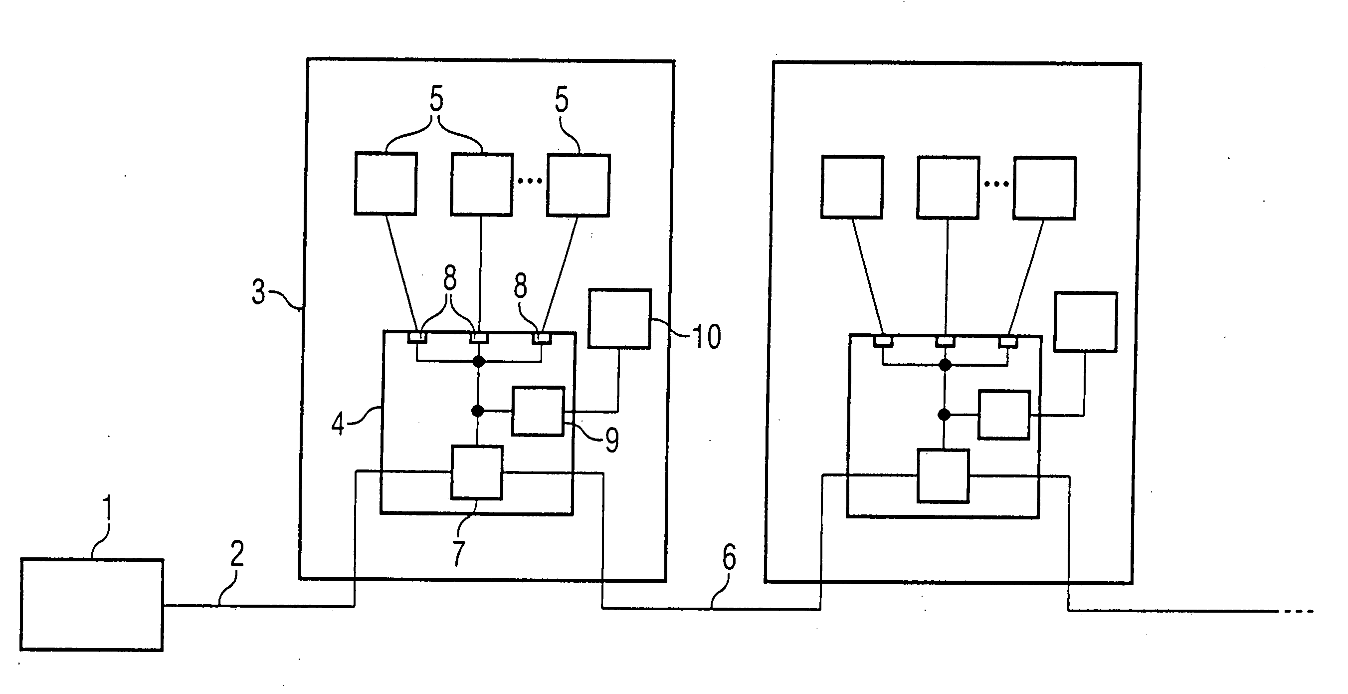
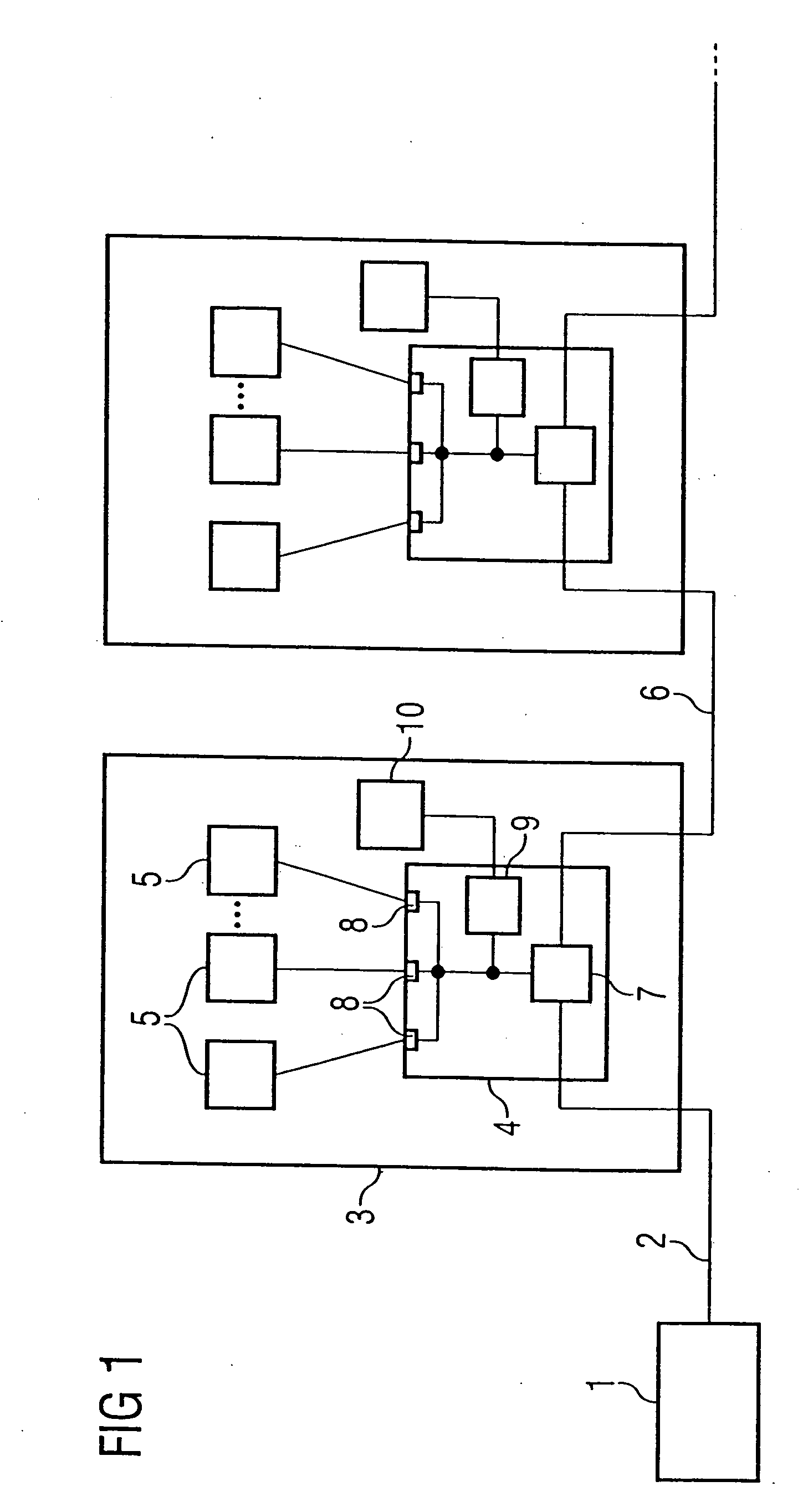
[0021]FIG. 1 shows a memory system, e.g., for a computer system, particularly a DDR memory system. The memory system has a memory controller 1 to which an address bus 2 with a number n of address lines is connected. The address lines are connected to an input of a memory module 3. The memory module 3 has a hub chip 4 to which one or more memory chips 5, e.g., DRAM memory chips, are connected. The number of connected memory chips 5 is determined by the address space which is to be formed. The address input of the memory module 3 is connected to an address input of the hub chip 4. The hub chip 4 has an address output which is connected to a further address bus 6 via the address output of the memory module 3. The further address bus 6 is connected to an address input of a further memory module.

[0022] The hub chip 4 has an address decoder unit 7 which checks the addresses which are present on the address bus 2 and, depending on the address applied, addresses the relevant connected memo...


PUM


Abstract

The invention relates to a hub chip for connecting one or more memory chips via a respective memory chip interface, having an address input for connecting the hub chip to an address bus and having an address output for connection to a further address bus, having an address decoder unit configured to use an address applied to the address input to address one of the connected memory chips or to apply the applied address to the address output, characterized by an error recognition unit configured to use provided checking data to detect an error in a memory area of the one or more memory chips.

Description

CROSS-REFERENCE TO RELATED APPLICATIONS [0001] This application is a continuation of co-pending PCT patent application No. PCT / EP 2004 / 008783, filed Aug. 5, 2004, which claims the benefit of German patent application serial number DE 103 35 978.8, filed Aug. 6, 2003. Each of the aforementioned related patent applications is herein incorporated by reference in its entirety. BACKGROUND OF THE INVENTION [0002] 1. Field of the Invention [0003] The invention relates to a hub chip for connecting one or more memory chips in a memory system. [0004] 2. Description of the Related Art [0005] Memory chips are frequently used in personal computers in order to store data for processing in the personal computer. The memory chips are usually combined to form memory modules in order to increase the storage capacity. To use the storage capacity of a plurality of memory modules, an address and data bus is usually provided which has the memory modules connected to it in parallel, i.e., each of the memo...

Claims


Application Information

Patent Timeline
IPC IPC(8): G06F12/14G11C8/00
CPCG11C8/00G06F12/00G06F12/02G11C29/52
Inventor POECHMUELLER, PETER
Owner INFINEON TECH AG
Learn More