
Multilayer printed wiring board and a process of producing same

a printing process and wiring board technology, applied in the direction of printing element electric connection formation, insulating substrate metal adhesion improvement, transportation and packaging, etc., can solve the problems of difficult to form a small diameter through hole, difficult to enhance and difficult to form a high-density wiring pattern, etc., to achieve the effect of increasing the density of the wiring pattern

Inactive Publication Date: 2006-08-31
HOYA CORP
View PDF24 Cites 27 Cited by
  • Summary
  • Abstract
  • Description
  • Claims
  • Application Information

AI Technical Summary

Benefits of technology

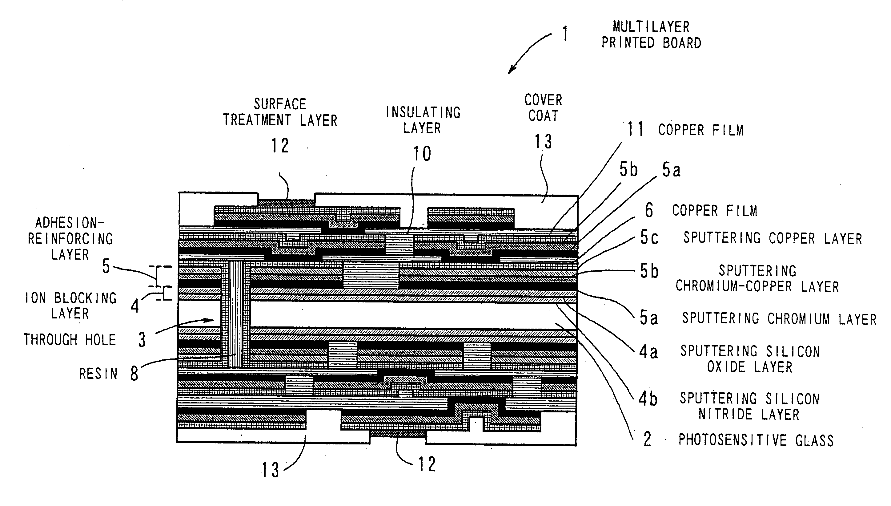
[0012] The present invention was created in view of the above circumstances, and an object thereof is to provide a multilayer printed wiring board which permits the formation of fine wiring patterns, thereby increasing the density of wiring patterns.
[0013] It is another object of the present invention to provide a process of producing a multilayer printed wiring board which permits the formation of fine wiring patterns, thereby increasing the density of wiring patterns.

Problems solved by technology

In the case of the ceramic wiring board, however, since the wiring pattern is printed on a green sheet, it is difficult to form a high-density wiring pattern.
Further, in the ceramic wiring board, a through hole is formed by punching, and thus it is difficult to form a small-diameter through hole.
As a result, the land has an increased width corresponding to the diameter of the through hole, also making it difficult to enhance the density of the wiring pattern.
When such a thick copper film is etched, the amount of side etching tends to increase, giving rise to a problem that the wiring of the core layer cannot be made fine.
Further, in the buildup wiring board, a through hole is formed by drilling, and thus it is difficult to form a through hole with a diameter of 0.3 mm or less.
As a result, the land has an increased width corresponding to the diameter of the through hole, also making it difficult to enhance the density of the wiring pattern.

Method used


Image

  • Multilayer printed wiring board and a process of producing same
  • Multilayer printed wiring board and a process of producing same
  • Multilayer printed wiring board and a process of producing same

Examples


example 1

[0090] An example according to the first embodiment will be now described.

[0091] In this example, a photosensitive glass (trade name: PEG3, manufactured by HOYA CORPORATION) having the composition stated below was used as the glass substrate.

[0092] (wt %)

SiO278.0%Li2O10.0%Al2O3 6.0%K2O 4.0%Na2O 1.0%ZnO 1.0%Au0.003% Ag0.08%CeO20.08%

(Through Hole Formation Step)

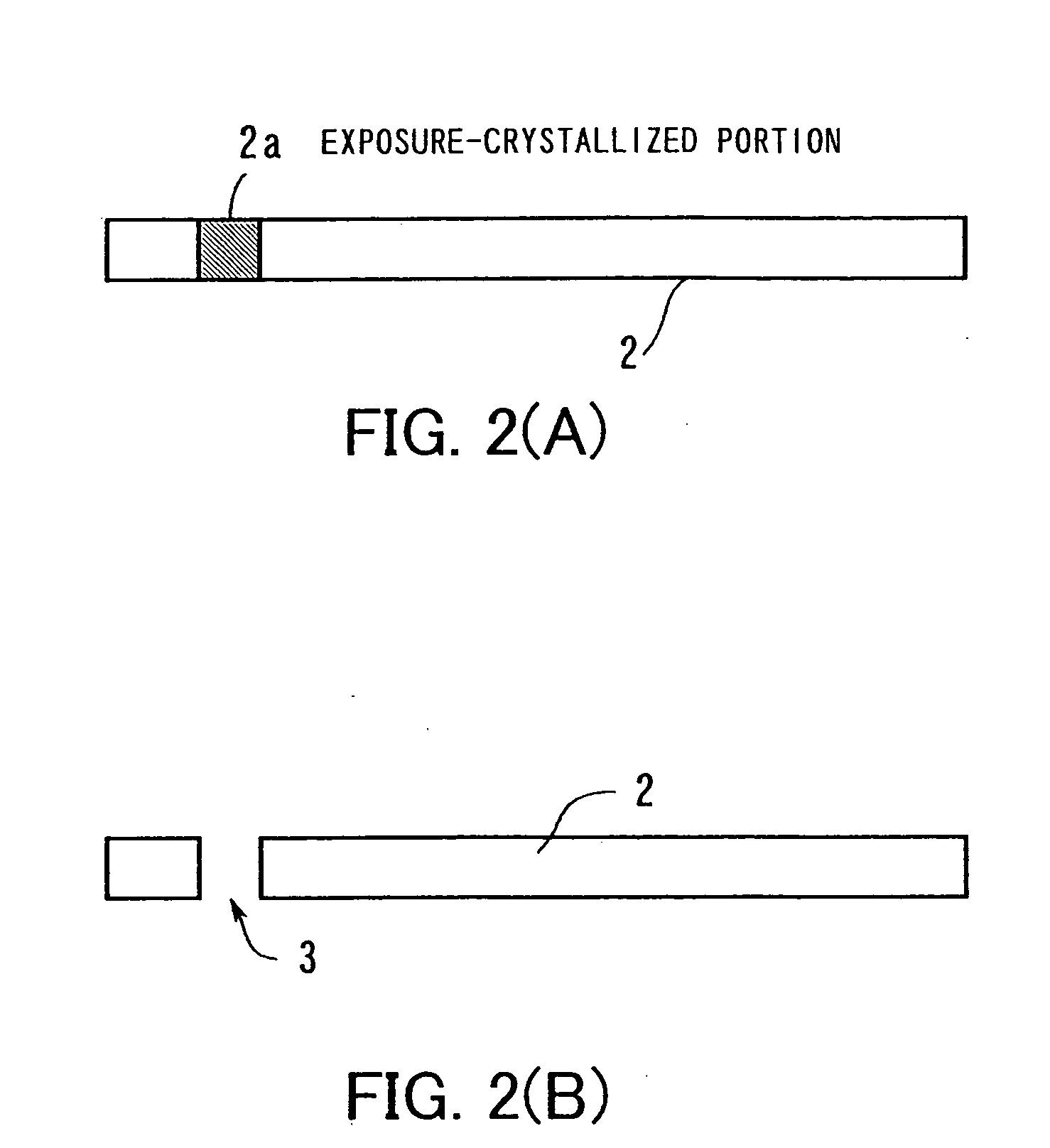
[0093] 1) With a mask held in close contact with the photosensitive glass, UV light was irradiated onto a through hole portion of the glass through the mask, thereby forming a latent image corresponding to the exposed portion. The mask used was made of silica glass patterned using chromium / chromium oxide. Subsequently, the photosensitive glass was heat-treated at 400° C. to crystallize only the exposed portion.

[0094] 2) Dilute hydrofluoric acid (10% solution) was sprayed on both surfaces of the photosensitive glass to remove the crystallized through hole portion by dissolution, thereby forming a through hole with a diame...


PUM

PropertyMeasurementUnit
thicknessaaaaaaaaaa
thicknessaaaaaaaaaa
thicknessaaaaaaaaaa

Abstract

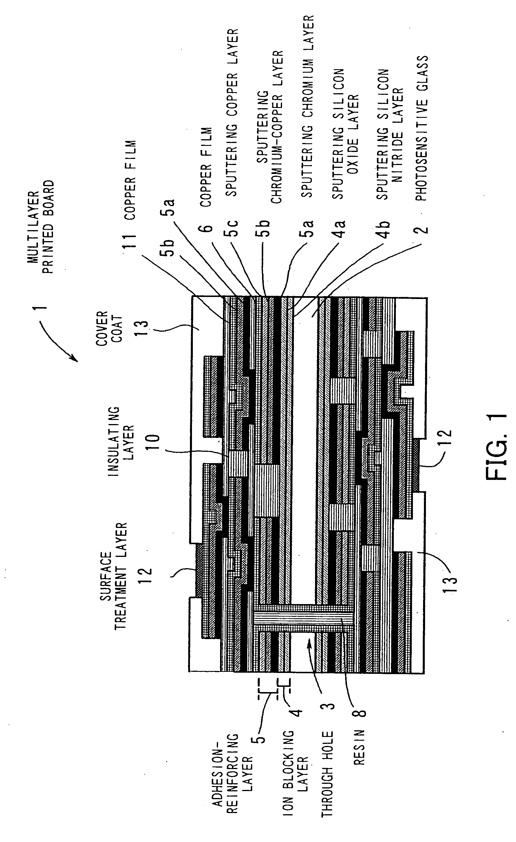
A multilayer printed wiring board which permits the formation of fine wiring patterns, thereby increasing the density of wiring patterns. Using photosensitive glass having a coefficient of thermal expansion close to that of a copper film as a core substrate, a through hole is formed in the photosensitive glass by photolithography, a sputtering silicon oxide layer and a sputtering silicon nitride layer are formed to prevent leak of alkali metal ions from the photosensitive glass, a sputtering chromium layer, a sputtering chromium-copper layer and a sputtering copper layer are formed to enhance the adhesion strength between the copper film and the sputtering silicon oxide layer, and a copper film of 1 to 20 μm thick is formed. With resin filled into the interior of the through hole, a wiring layer is patterned by etching, an insulating layer is formed, and the surface is covered with a surface treatment layer and a cover coat.

Description

[0001] This application is a divisional of application Ser. No. 11 / 209,790 filed Aug. 24, 2005, which is a divisional of application Ser. No. 10 / 003,103 filed on Dec. 6, 2001, which has been abandoned, which is a divisional application of Ser. No. 09 / 579,270, filed May 26, 2000, issued as U.S. Pat. No. 6,339,197 on Jan. 15, 2002.BACKGROUND OF THE INVENTION [0002] (1) Field of the Invention [0003] The present invention relates to a multilayer printed wiring board having a multilayer wiring pattern and a process of producing same, and more particularly, to a multilayer printed wiring board which permits the formation of high-density wiring patterns and a production process therefor. [0004] (2) Description of the Related Art [0005] In recent years, MCM (Multi Chip Module) having a plurality of bare-chip LSIs mounted at high density on a multilayer wiring board has come to be widely used. MCM is used in various types of OA equipment, mobile communication equipment, industrial equipment,...

Claims


Application Information

Patent Timeline
Patent Type & Authority Applications(United States)
IPC IPC(8): H05K1/03H05K3/28H01L23/538H05K3/00H05K3/18H05K3/38H05K3/42H05K3/46
CPCH01L23/5384Y10T428/24926H05K1/0306H05K3/388H05K3/426H05K3/4602H05K3/4605H05K3/467H05K2201/0154H05K2201/0175H05K2201/0179H05K2201/068H05K2201/09536H05K2201/0959H01L2924/0002H01L2924/09701Y10T29/49165H01L2924/00
Inventor FUSHIE, TAKASHIKAGATSUME, TAKESHIMATSUI, SHIGEKAZU
Owner HOYA CORP
Learn More