Surface emitting type device, and method for manufacturing the same

a surface emitting and type technology, applied in the direction of photoelectric discharge tubes, semiconductor lasers, instruments, etc., can solve the problems of low tolerance to reverse bias voltage, device damage, device destruction, etc., to prevent electrostatic destruction and improve reliability.

Inactive Publication Date: 2006-08-31
SEIKO EPSON CORP
View PDF6 Cites 7 Cited by
  • Summary
  • Abstract
  • Description
  • Claims
  • Application Information

AI Technical Summary

Benefits of technology

[0006] In accordance with an advantage of some aspects of the invention, electrostatic destruction can be prevented and reliability can be improved with respect to surface-emitting type devices and methods for manufacturing the same.

Problems solved by technology

For this reason, the device may be damaged by static electricity caused by a machine or an operator in a mounting process.
In particular, a surface-emitting type device such as a surface-emitting type semiconductor laser has a certain tolerance to a forward bias voltage, but has a low tolerance to a reverse bias voltage, and the device may be destroyed when a reverse bias voltage is impressed.
A variety of measures are usually implemented in a mounting process to remove static electricity, but these measures have limitations.

Method used


Image

  • Surface emitting type device, and method for manufacturing the same
  • Surface emitting type device, and method for manufacturing the same
  • Surface emitting type device, and method for manufacturing the same

Examples


first embodiment

1. First Embodiment

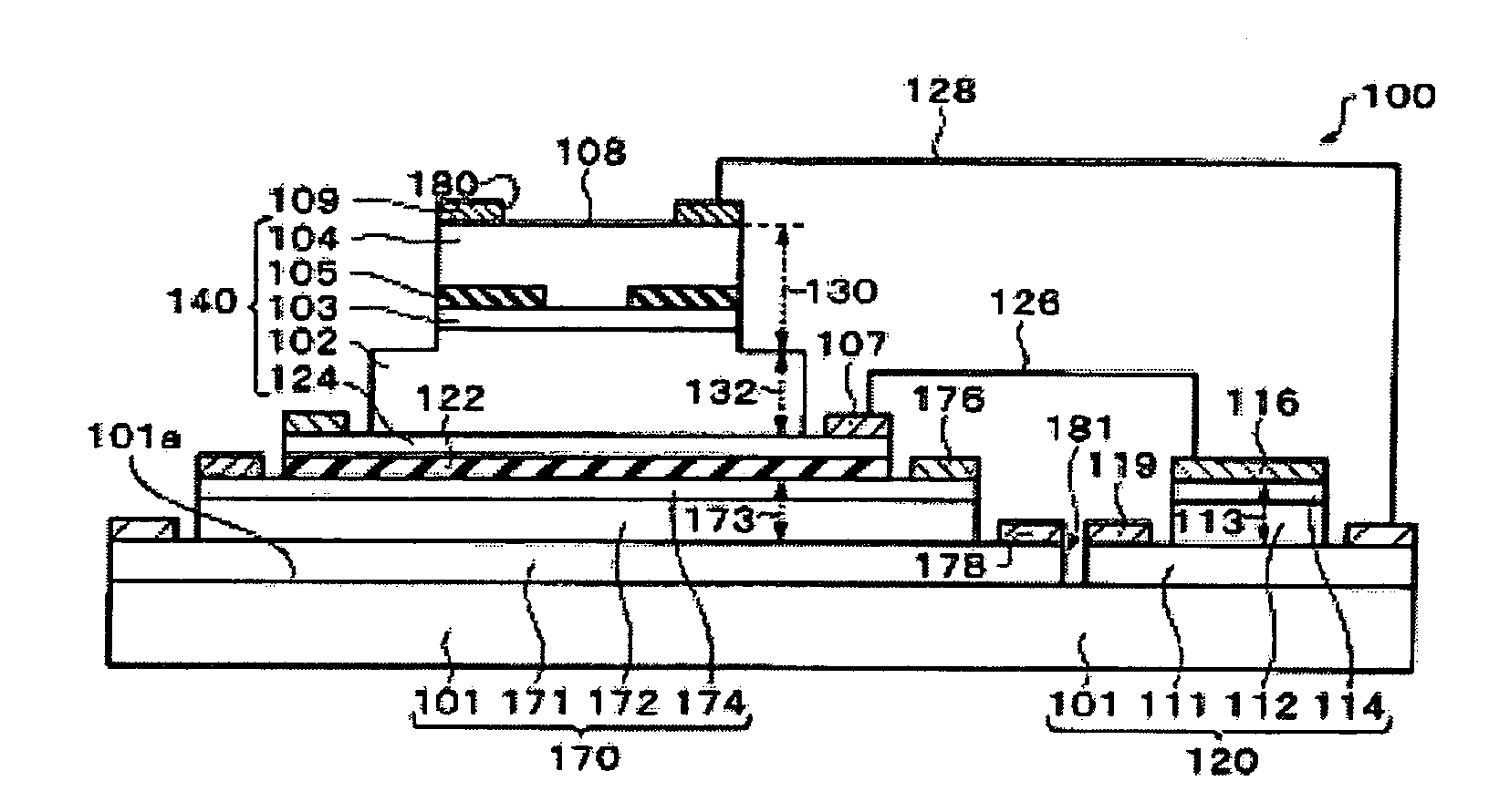
[0037] 1-1. First, a surface-emitting type device 100 in accordance with a first embodiment is described.

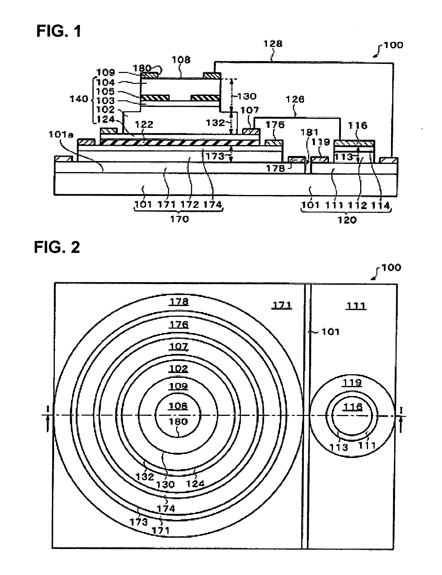
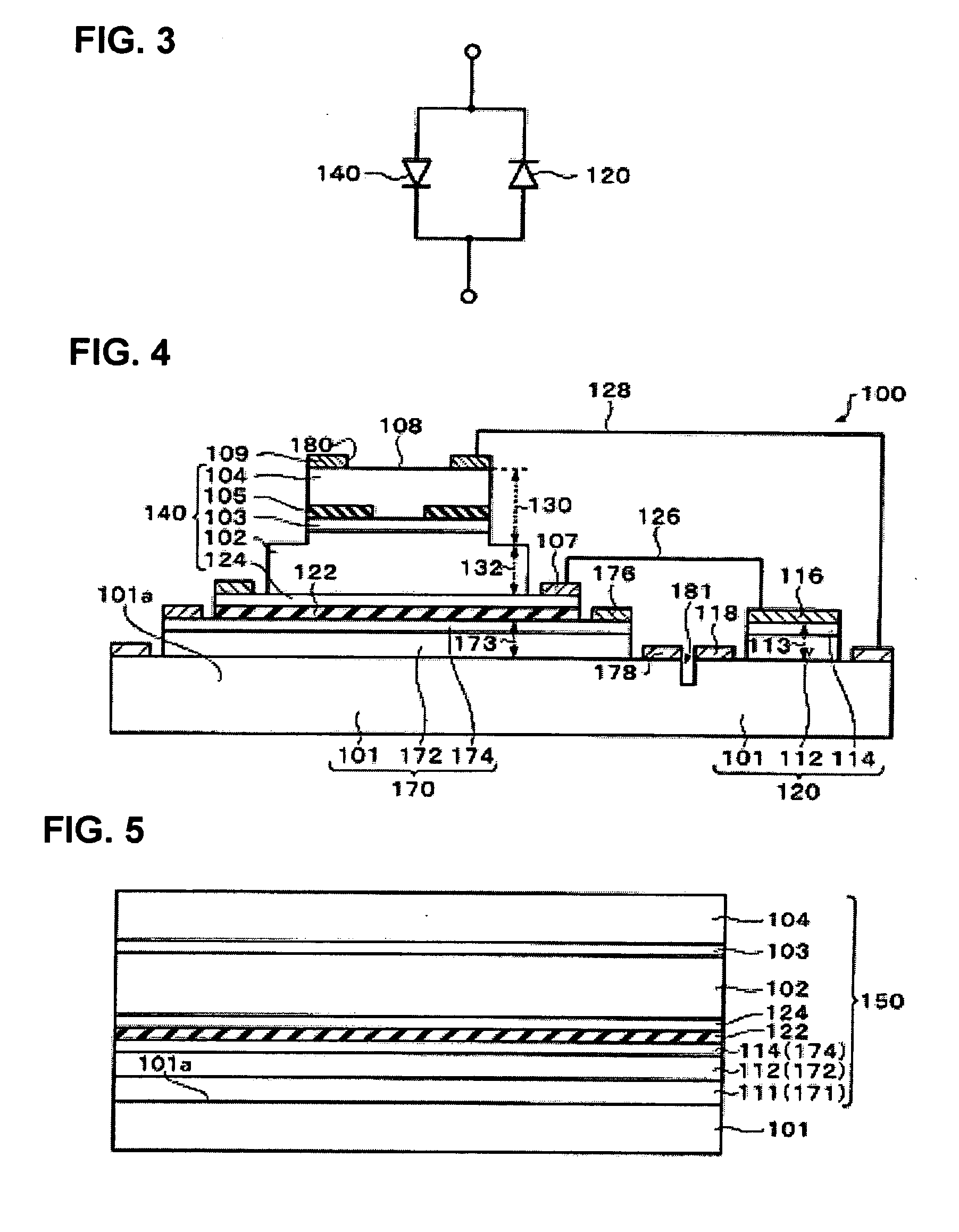
[0038]FIG. 1 is a cross-sectional view taken along a line I-I of FIG. 2, and FIG. 2 is a plan view schematically showing the surface-emitting type device 100. FIG. 3 is a circuit diagram of a main portion of the surface-emitting type device 100.

[0039] The surface-emitting type device 100 includes, as shown in FIG. 1 and FIG. 2, a rectification section 120, an emission section 140 and a photodetector section 170. The present embodiment is described as to a case in which the rectification section 120 functions as a junction diode (including a Zener diode), the emission section 140 functions as a surface-emitting type semiconductor laser, and the photodetector section 170 functions as a photodiode.

[0040] The rectification section 120 includes a substrate 101, a fourth semiconductor layer 111 formed above the substrate 101, a capacitance adjusting layer 112 form...

second embodiment

2. Second Embodiment

[0074] 2-1. Next, a surface-emitting type device 200 in accordance with a second embodiment is described. It is noted that features different from the surface-emitting type device 100 described above and shown in FIG. 1 and FIG. 2 are mainly described, and descriptions of similar features are omitted.

[0075]FIG. 7 is a cross-sectional view taken along a line VIII-VIII of FIG. 8, and FIG. 8 is a plan view schematically showing the surface-emitting type device 200. It is noted that the same members as those of the surface-emitting type device 100 described above and shown in FIG. 1 and FIG. 2 are appended with the same reference numbers.

[0076] The surface-emitting type device 200 includes a rectification section 120, an emission section 140, a photodetector section (hereafter referred to as a “first photodetector section”) 170, and another photodetector section (hereafter referred to as a “second photodetector section”), as shown in FIG. 8 and FIG. 9. The present ...


PUM


Abstract

A surface-emitting type device includes a rectification section including a substrate and a first semiconductor layer formed above the substrate, an emission section including a second semiconductor layer of a first conductivity type formed above the rectification section, an active layer formed above the second semiconductor layer and a third semiconductor layer of a second conductivity type formed above the active layer, and a photodetection section including the substrate, a photoabsorption layer formed above the substrate and a contact layer formed above the photoabsorption layer, wherein the first semiconductor layer and the contact layer are formed by a common process, the rectification section and the emission section are electrically connected in parallel with each other, and the rectification section has a rectification action in a reverse direction with respect to the emission section.

Description

[0001] The entire disclosure of Japanese Patent Application No. 2005-029233, filed Feb. 4, 2005 is expressly incorporated by reference herein. BACKGROUND [0002] 1. Technical Field [0003] The present invention relates to surface-emitting type devices and methods for manufacturing the same. [0004] 2. Related Art [0005] A surface-emitting type semiconductor laser has a smaller device volume compared to an ordinary edge-emitting type semiconductor laser, such that the electrostatic breakdown voltage of the device itself is low. For this reason, the device may be damaged by static electricity caused by a machine or an operator in a mounting process. In particular, a surface-emitting type device such as a surface-emitting type semiconductor laser has a certain tolerance to a forward bias voltage, but has a low tolerance to a reverse bias voltage, and the device may be destroyed when a reverse bias voltage is impressed. A variety of measures are usually implemented in a mounting process to...

Claims


Application Information

Patent Timeline
Patent Type & Authority Applications(United States)
IPC IPC(8): H01J40/14
CPCH01S5/0261H01S5/0262H01S5/0264H01S5/0425H01S5/06825H01S5/18311H01S5/18341H01S5/04256H01S5/04257
Inventor KOYAMA, TOMOKO
Owner SEIKO EPSON CORP
Why Eureka
Try Eureka