Solid-state imaging device

Inactive Publication Date: 2006-08-31
PANASONIC CORP
View PDF7 Cites 16 Cited by
  • Summary
  • Abstract
  • Description
  • Claims
  • Application Information

AI Technical Summary

Benefits of technology

[0013] Therefore, in order to solve the above described problems in the conventional amplification-type MOS image sensor, an object of the present invention is to provide a solid-state imaging device in which a

Problems solved by technology

Because a source follower output circuit comprises the amplification transistor 25 and a load transistor 26 which is disposed outside a pixel region, if a gain of the amplification transistor 25 fluctuates, sensitivity of pixels will fluctuate, causing noise and th

Method used


Image

  • Solid-state imaging device
  • Solid-state imaging device
  • Solid-state imaging device

Examples


first embodiment

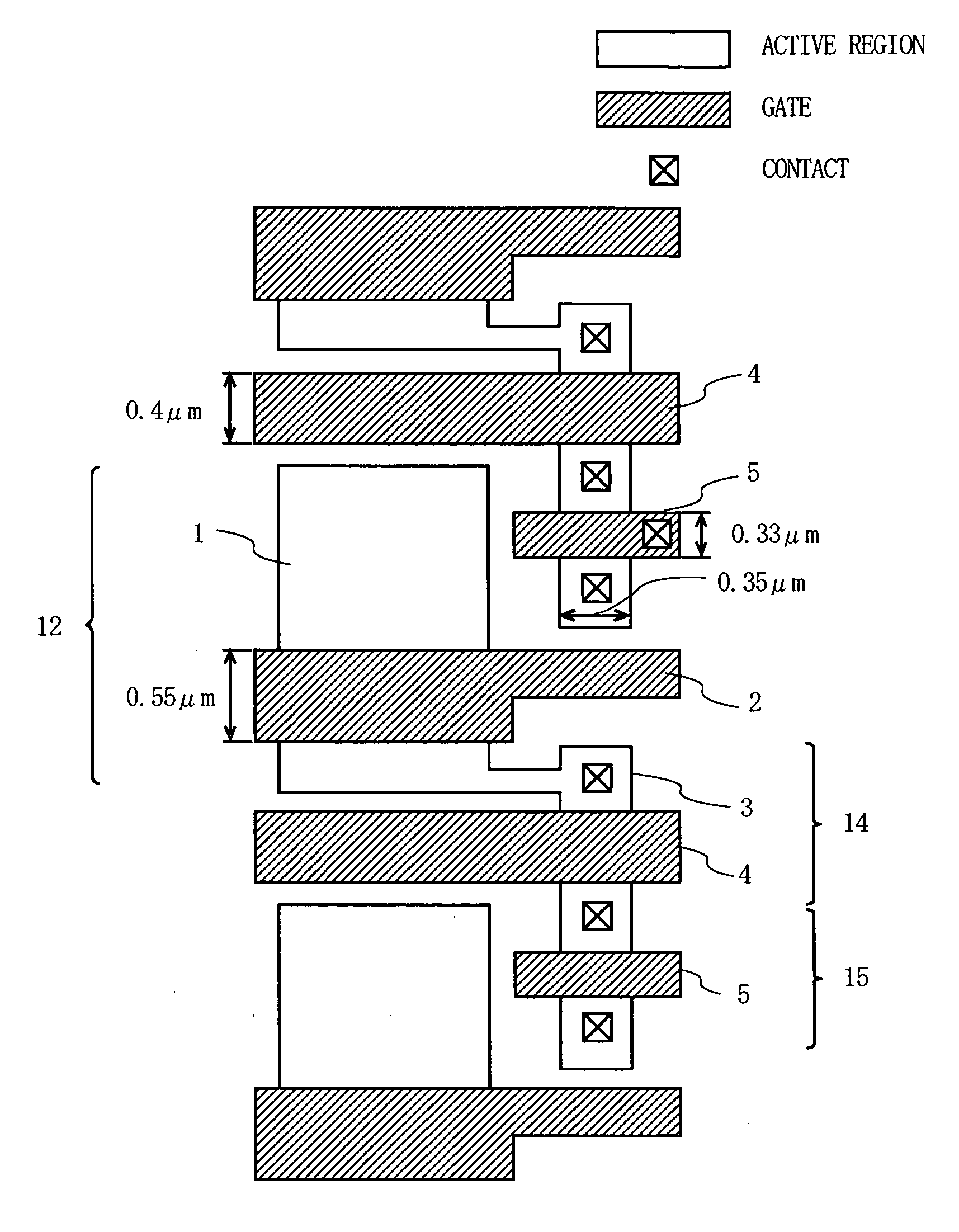
[0026]FIG. 1 is a plan view illustrating a pixel layout in a solid-state imaging device (MOS image sensor) according to a first embodiment of the present invention. More specifically, FIG. 1 shows a layout of active regions, gates, and contacts, and illustrates a layout, mainly, of a photodiode 1, a transfer gate 2 of a transfer transistor 12, a floating diffusion section 3 (hereinafter referred to as an FD section 3), reset gates 14 of are set transistor 14, and amplification gates 5 of an amplification transistor 15. Here, the transfer gate 2 is to transfer to the FD section 3 charges accumulated by the photodiode 1. The amplification gates 5 are electrically connected to the FD section 3. The reset transistor 14 is to reset a potential of the FD section 3.

[0027] As shown in FIG. 1, a physical gate length (hereinafter, simply referred to as a gate length) of the transfer gate 2 and a gate length of the reset gate 4 are, for example, 0.55 μm and 0.4 μm, respectively, and a gate le...

second embodiment

[0046]FIG. 5 shows the plan view of the layout of pixels in the solid-state imaging device (the MOS image sensor) according to the second embodiment of the present invention. A configuration of the solid-state imaging device according to the present embodiment is different from that according to the first embodiment in that only one FD section 3 is disposed for two transfer transistors 12a and 12b and two pixels neighboring above and below share an amplification transistor 15, a selection transistor 16, and a reset transistor 14.

[0047] Charges accumulated in the two photodiodes 1-a and 1-b are transferred to the FD section 3 when voltages are applied to respective transfer gates 2-a and 2-b. The FD section 3 is connected to the reset transistor 14 for resetting a FD potential. The FD section 3 is connected to an amplification gate 5 of the amplification transistor 15. The selection transistor 16 is connected to a drain side of the amplification transistor 15.

[0048] In the present ...


PUM


Abstract

Pixels have a photodiode 1, a transfer gate electrode 2 for transferring charges accumulated in the photodiode 1, a floating diffusion section 3 for accumulating the charge transferred by the transfer gate electrode 2, an amplification transistor 15 in which a gate electrode is connected to the floating diffusion section 3, and a reset transistor 14 for resetting a potential of the floating diffusion section 5. A gate length of the amplification transistor 15 is shorter than a gate length of a transistor, among transistors comprising the peripheral circuitry region, whose gate insulating film thickness is a same as a gate insulating film thickness of the amplification transistor 15 and which has a minimum gate length.

Description

BACKGROUND OF THE INVENTION [0001] 1. Field of the Invention [0002] The present invention relates to a solid-state imaging device having a plurality of photoelectric conversion elements disposed therein and more particularly, to a technique for enhancing sensitivity by noise reduction and for miniaturizing a pixel size. [0003] 2. Description of the Background Art [0004] In recent years, an amplification-type MOS image sensor has been utilized for coping with high voltage operations or the like. FIG. 7 shows a circuit configuration of pixels in the conventional amplification-type MOS image sensor, for example, disclosed in Japanese Laid-Open Patent Publication No. 2003-46865. [0005] The conventional MOS image sensor includes a photodiode 21, a transfer transistor 22 for transferring charges from the photodiode 21 to a floating diffusion section 23 (hereinafter, referred to as FD 23), are set transistor 24 for resetting a potential of the FD 23, and an amplification transistor 25 for ...

Claims


Application Information

Patent Timeline
IPC IPC(8): H01L31/113H01L27/146
CPCH01L27/14603H01L27/146
Inventor MIYAGAWA, RYOUHEI
Owner PANASONIC CORP
Why Eureka
Try Eureka