Magnetic elements with ballistic magnetoresistance utilizing spin-transfer and an MRAM device using such magnetic elements

a technology of magnetic elements and ballistic magnetoresistance, which is applied in the field of magnetic memory systems, can solve the problems of high signal output, power consumption, and the probability of nearby cells being inadvertently switched, and achieve the effect of high signal outpu

Inactive Publication Date: 2006-08-31
SAMSUNG SEMICON
View PDF0 Cites 56 Cited by
  • Summary
  • Abstract
  • Description
  • Claims
  • Application Information

AI Technical Summary

Benefits of technology

[0018] According to the system and method disclosed herein, the present invention provides a magnetic element that is preferably capable of being written using the more efficient and localized spin-transfer switching while providing a high signal output.

Problems solved by technology

Consequently, cross talk, power consumption, and the probability that nearby cells will be inadvertently switched may increase.
The driving circuits used to drive the current that generates the switching field could also increase in area and complexity.
This upper limit on the write current amplitude can lead to reliability issues because some cells are harder to switch than others (due to fabrication and material nonuniformity) and may fail to write consistently.
Ballistic MR results in a large fractional change in resistance between two magnetic regions having different orientations of magnetization.
Consequently, ballistic MR does not typically contribute to the resistance of a magnetic material because the reflections of electrons at the domain wall are negligible.
In such a case, many of the drawbacks of conventional magnetic elements, such as the magnetic element 10 and 10′, are still present.

Method used


Image

  • Magnetic elements with ballistic magnetoresistance utilizing spin-transfer and an MRAM device using such magnetic elements
  • Magnetic elements with ballistic magnetoresistance utilizing spin-transfer and an MRAM device using such magnetic elements
  • Magnetic elements with ballistic magnetoresistance utilizing spin-transfer and an MRAM device using such magnetic elements

Examples


second embodiment

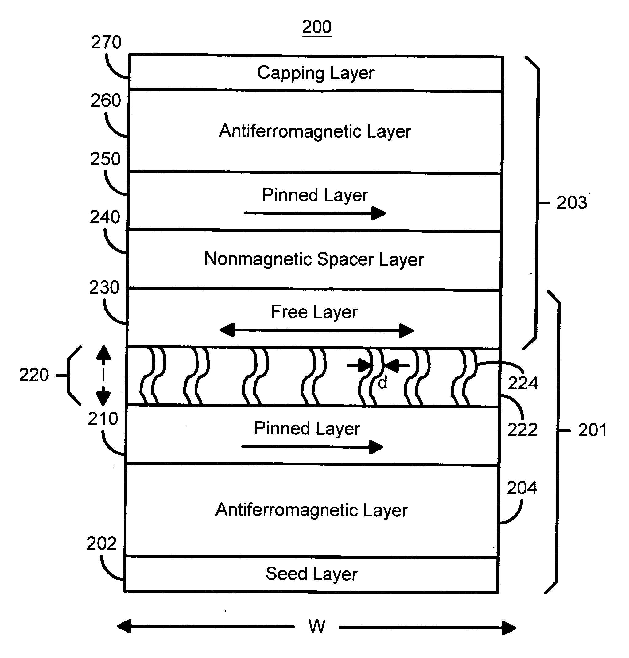
[0037]FIG. 4 is a diagram depicting a magnetic element 200 having a magnetic current confined layer in accordance with the present invention. The magnetic element 200 has components which are analogous to those of the magnetic element 100 depicted in FIG. 3. Consequently, these elements are labeled similarly. The magnetic element 200 thus includes a ferromagnetic pinned layer 210, a ferromagnetic free layer 230, and a magnetic current confined layer 220 having ferromagnetic conductive channels 224 in an insulating matrix 222. In addition, the lengths and diameters of the ferromagnetic conductive channels 224 are such that ballistic MR can be exhibited by the magnetic element 200. Stated differently, the sizes of the conductive channels 224 are such that charge carriers passing through the magnetic element 200 in a CPP configuration can give rise to ballistic MR. The ferromagnetic conductive channels 224 preferably include Ni, Fe, Co or their alloys. The insulating matrix 222 prefera...


PUM

PropertyMeasurementUnit
thicknessaaaaaaaaaa
diameteraaaaaaaaaa
depthaaaaaaaaaa

Abstract

A method and system for providing a magnetic element is disclosed. The method and system include providing a pinned layer, a magnetic current confined layer, and a free layer. The pinned layer is ferromagnetic and has a first pinned layer magnetization. The magnetic current confined layer has at least one channel in an insulating matrix and resides between the pinned layer and the free layer. The channel(s) are ferromagnetic, conductive, and extend through the insulating matrix between the free layer and the pinned layer. The size(s) of the channel(s) are sufficiently small that charge carriers can give rise to ballistic magnetoresistance in the magnetic current confined layer. The free layer is ferromagnetic and has a free layer magnetization. Preferably, the method and system also include providing a second pinned layer and a nonmagnetic spacer layer between the second pinned layer and the free layer. In this aspect, the magnetic element is configured to allow the free layer magnetization to be switched using spin transfer.

Description

CROSS-REFERENCE TO RELATED APPLICATIONS [0001] The present application is a divisional of co-pending U.S. patent application Ser. No. 10 / 745,151 filed on Dec. 22, 2003, entitled “MAGNETIC ELEMENTS WITH BALLISTIC MAGNETORESISTANCE UTILIZING SPIN-TRANSFER AND AN MRAM DEVICE USING SUCH MAGNETIC ELEMENTS” and assigned to the assignee of the present application.FIELD OF THE INVENTION [0002] The present invention relates to magnetic memory systems, and more particularly to a method and system for providing an element that employs a spin transfer effect in switching and that can be used in a magnetic memory such as magnetic random access memory (“MRAM”). BACKGROUND OF THE INVENTION [0003]FIGS. 1A and 1B depict conventional magnetic elements 10 and 10′. The conventional magnetic element 1 is a spin valve 10 and includes a conventional antiferromagnetic (AFM) layer 12, a conventional pinned layer 14, a conventional nonmagnetic spacer layer 16 and a conventional free layer 18. The conventiona...

Claims


Application Information

Patent Timeline
Patent Type & Authority Applications(United States)
IPC IPC(8): H01L29/94H01L27/108H01L29/76H01L31/119G11C11/15G11C11/16H01F10/32H01F41/30H01L21/336H01L43/08H01L43/12
CPCB82Y25/00B82Y40/00G11C11/16H01F10/3227H01F10/3254H01F10/3259H01F41/305H01L43/08H01L43/12H01F10/3295H01F10/3272H10N50/10H10N50/01
Inventor HUAI, YIMING
Owner SAMSUNG SEMICON
Why Eureka
Try Eureka