Piezoelectric cantilever beam sensor structure and manufacturing method thereof

A manufacturing method and technology of cantilever beams, applied in the manufacture/assembly of piezoelectric/electrostrictive devices, piezoelectric/electrostrictive/magnetostrictive devices, circuits, etc., can solve the problems of low sensitivity, difficult control and complicated process and other issues, to achieve the effect of improving response and signal output, simplifying structure and processing technology, and making the process simple and controllable

Inactive Publication Date: 2016-04-20
SHANGHAI INTEGRATED CIRCUIT RES & DEV CENT +1
View PDF6 Cites 8 Cited by
  • Summary
  • Abstract
  • Description
  • Claims
  • Application Information

AI Technical Summary

Problems solved by technology

However, there are very few piezoelectric microdevices that can be applied in practice. The key problems are: first, the microfabrication technology of piezoelectric thin films and the compatibility between piezoelectric thin films and silicon integrated circuit technology have not been well resolved. The second is that most of the piezoelectric sensors use bulk silicon technology, and the release of the microstructure adopts the backside etching process of the silicon substrate. The process is complicated and difficult to control. The problem of bottom adhesion leads to a decrease in yield; third, most of the applied piezoelectric microdevices use rigid support structures such as polysilicon and piezoelectric ceramics, which are not sensitive to small-signal excitation and have low sensitivity; at the same time, those with rigid support structures Microdevices cannot be applied to objects of any size and any shape of surface

Method used


Image

  • Piezoelectric cantilever beam sensor structure and manufacturing method thereof
  • Piezoelectric cantilever beam sensor structure and manufacturing method thereof
  • Piezoelectric cantilever beam sensor structure and manufacturing method thereof

Examples


Embodiment Construction

[0029] The specific embodiment of the present invention will be further described in detail below in conjunction with the accompanying drawings.

[0030] It should be noted that, in the following specific embodiments, when describing the embodiments of the present invention in detail, in order to clearly show the structure of the present invention for the convenience of description, the structures in the drawings are not drawn according to the general scale, and are drawn Partial magnification, deformation and simplification are included, therefore, it should be avoided to be interpreted as a limitation of the present invention.

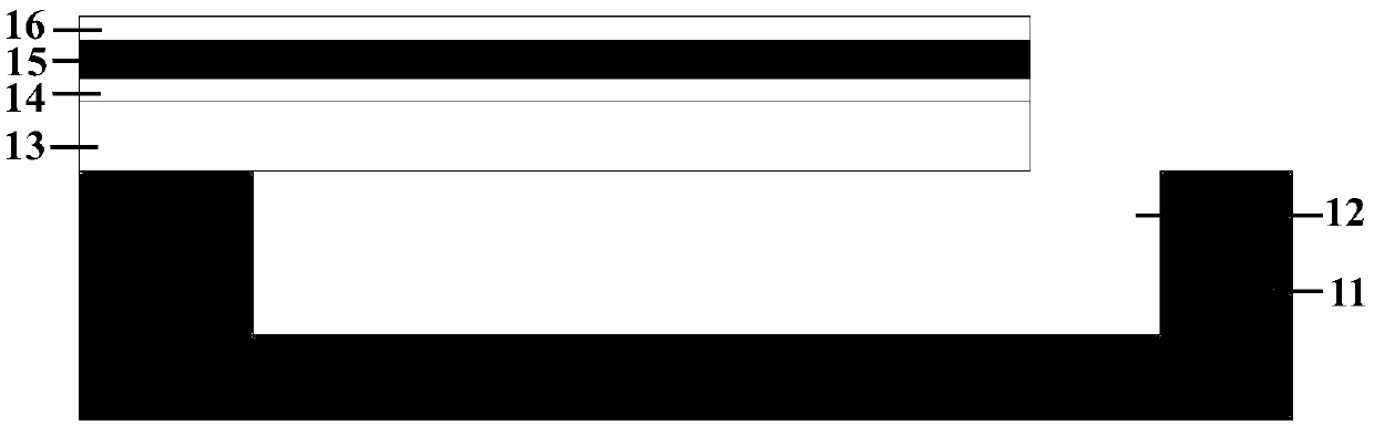
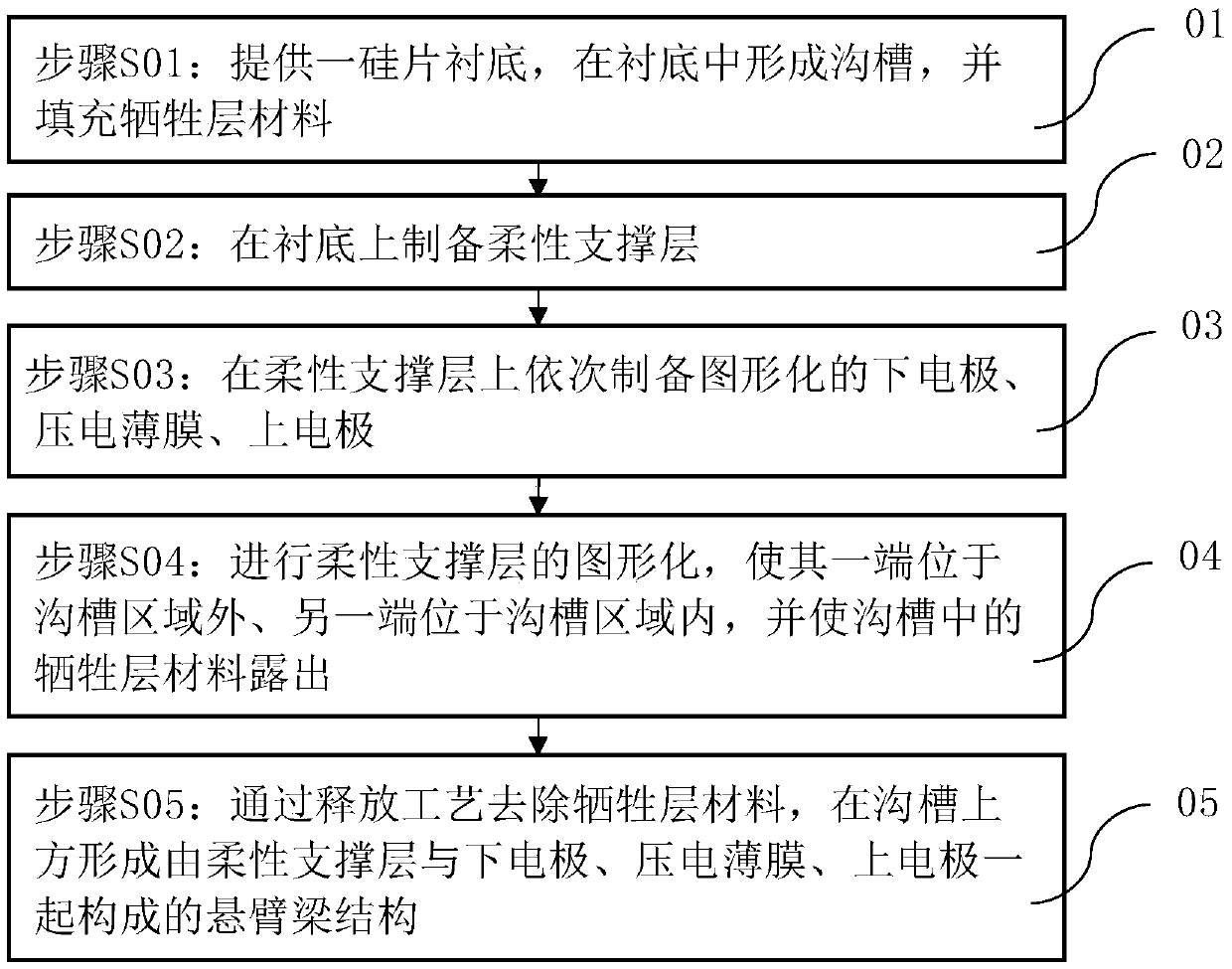
[0031] In the following specific embodiments of the present invention, please refer to figure 1 , figure 1 It is a structural schematic diagram of a piezoelectric cantilever beam sensor in a preferred embodiment of the present invention. like figure 1 As shown, a piezoelectric cantilever sensor structure of the present invention is built on a sili...


PUM


Abstract

The invention discloses a piezoelectric cantilever beam sensor structure. By taking a flexible material as a cantilever beam support structure, the sensor structure and the processing technology are simplified, the sensitivity of a sensor or the deformation amplitude of a performer can be substantially improved, and response and signal output of a cantilever beam for external excitation are improved. The invention also discloses a manufacturing method of a piezoelectric cantilever beam sensor structure. By use of a surface sacrificial layer technology and an isotropy wet-method etching technology, a piezoelectric micro-cantilever structure is released from the front side, the process is simple and controllable, the compatibility between the piezoelectric cantilever beam sensor manufacturing technology and a silicon integrated circuit technology can be improved, and the problem of pollution is avoided.

Description

technical field [0001] The present invention relates to the technical field of piezoelectric thin film microsensors, and more particularly relates to a piezoelectric cantilever beam sensor structure with flexible support and a manufacturing method thereof. Background technique [0002] The principle of piezoelectricity is a new way to realize microsensors. Through the piezoelectric effect, the perceived quantities such as force and acceleration can directly output voltage on the piezoelectric film, and the inverse piezoelectric effect enables the microsensor to drive the microstructure to generate displacement by applying an external voltage, so as to have the function of an actuator at the same time. The data show that microsensors / actuators made of piezoelectric thin film materials have unparalleled advantages compared with existing silicon-based microsensors / actuators, and are a new field of research and development for microsensors. [0003] The sensor based on the piez...

Claims


Application Information

Patent Timeline
Patent Type & Authority Applications(China)
IPC IPC(8): H01L41/053H01L41/113H01L41/27H01L41/332
CPCH10N30/88H10N30/306H10N30/302H10N30/05H10N30/082
Inventor 杨冰周伟肖慧敏
Owner SHANGHAI INTEGRATED CIRCUIT RES & DEV CENT
Why Eureka
Try Eureka