Magnetic memory cell, magnetic memory device, and method of manufacturing magnetic memory device

a magnetic memory device and memory cell technology, applied in semiconductor devices, digital storage, instruments, etc., can solve the problems of insufficient to achieve improved storage speed and access speed, insufficient to realize magnetic memory devices with higher packing density, and difficulty in performing sufficiently stable writing, etc., to achieve processing with high alignment precision and simplify the whole manufacturing process

Inactive Publication Date: 2007-11-13
TDK CORPARATION
View PDF12 Cites 7 Cited by
  • Summary
  • Abstract
  • Description
  • Claims
  • Application Information

AI Technical Summary

Benefits of technology

[0012]The present invention has been achieved in consideration of such problems and a first object of the invention is to provide a magnetic memory device capable of reducing a loss of a magnetic field generated by currents flowing in a write line and performing stable writing with a compact configuration, and a magnetic memory cell to be mounted on the magnetic memory device. A second object is to provide a magnetic memory device hardly exerting an adverse influence on an adjacent magnetic memory cell and a magnetic memory cell to be mounted on the magnetic memory device. A third object is to provide a high-speed and large-capacity magnetic memory device capable of obtaining a high signal output by using a pair of magnetoresistive devices and a magnetic memory cell to be mounted on the magnetic memory device. Further, a fourth object is to provide a method for easily manufacturing such a magnetic memory device.

Problems solved by technology

However, it is insufficient to achieve improvement in storing speed and access speed.
However, since an output voltage of even the MRAM using the TMR device achieving a resistance change rate of about 40% is tens mV, it is insufficient to realize a magnetic memory device of higher packing density.
In such an MRAM of the type in which the write bit line 105 and the write word line 106 are orthogonal to each other, the magnetization direction of the second magnetic layer 104 functioning as a free layer cannot be sufficiently maintained as a whole, and it is difficult to perform sufficiently stable writing.
Since the current magnetic field is an open magnetic field (which is not magnetically confined in a specific area), the efficiency is low and an adverse influence on neighboring memory cells is also concerned.
However, it is feared that demagnetizing field increases as the aspect ratio (thickness / width in the direction in the stack layer plane) of each of the magnetic layers in the TMR device becomes higher, the magnetic field intensity to change the magnetization direction of the free layer increases, and larger write current is necessary.

Method used


Image

  • Magnetic memory cell, magnetic memory device, and method of manufacturing magnetic memory device
  • Magnetic memory cell, magnetic memory device, and method of manufacturing magnetic memory device
  • Magnetic memory cell, magnetic memory device, and method of manufacturing magnetic memory device

Examples


first embodiment

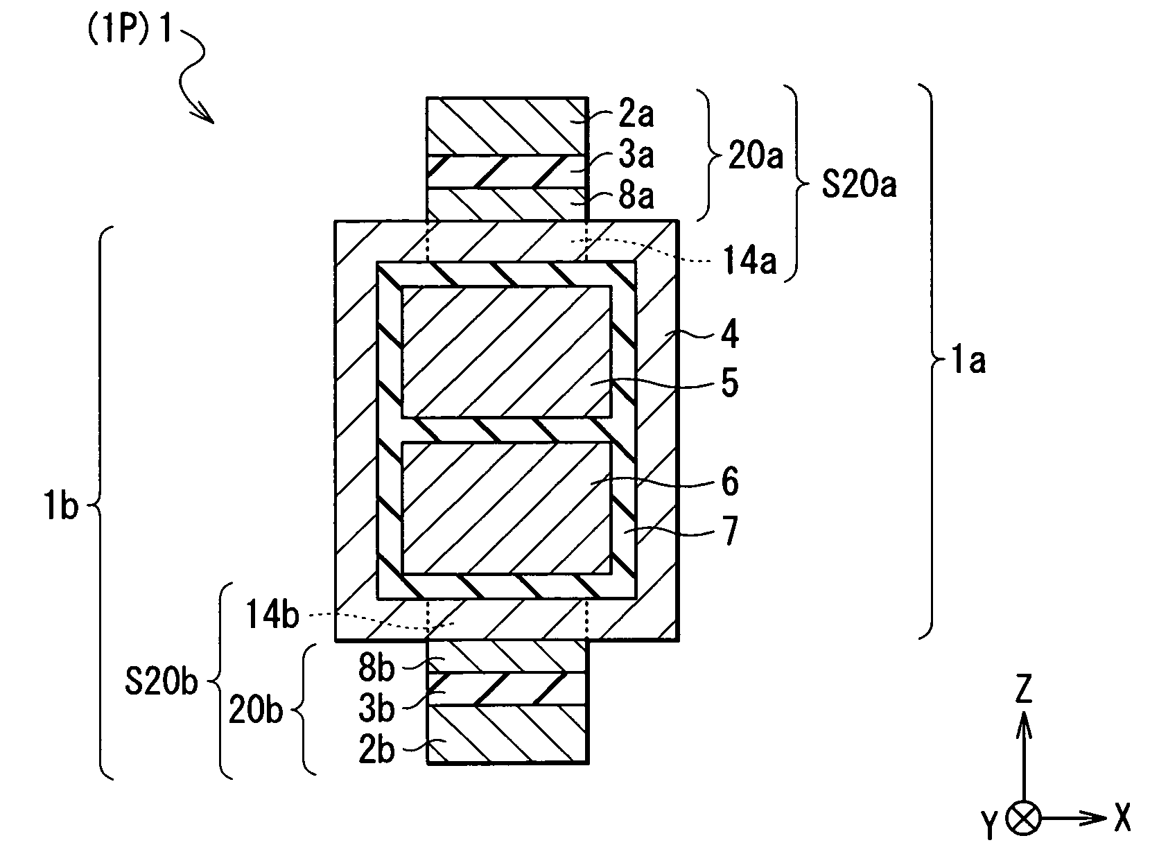
[0085]First, by referring to FIGS. 1 to 7, the configuration of a magnetic memory device according to a first embodiment of the invention will be described.

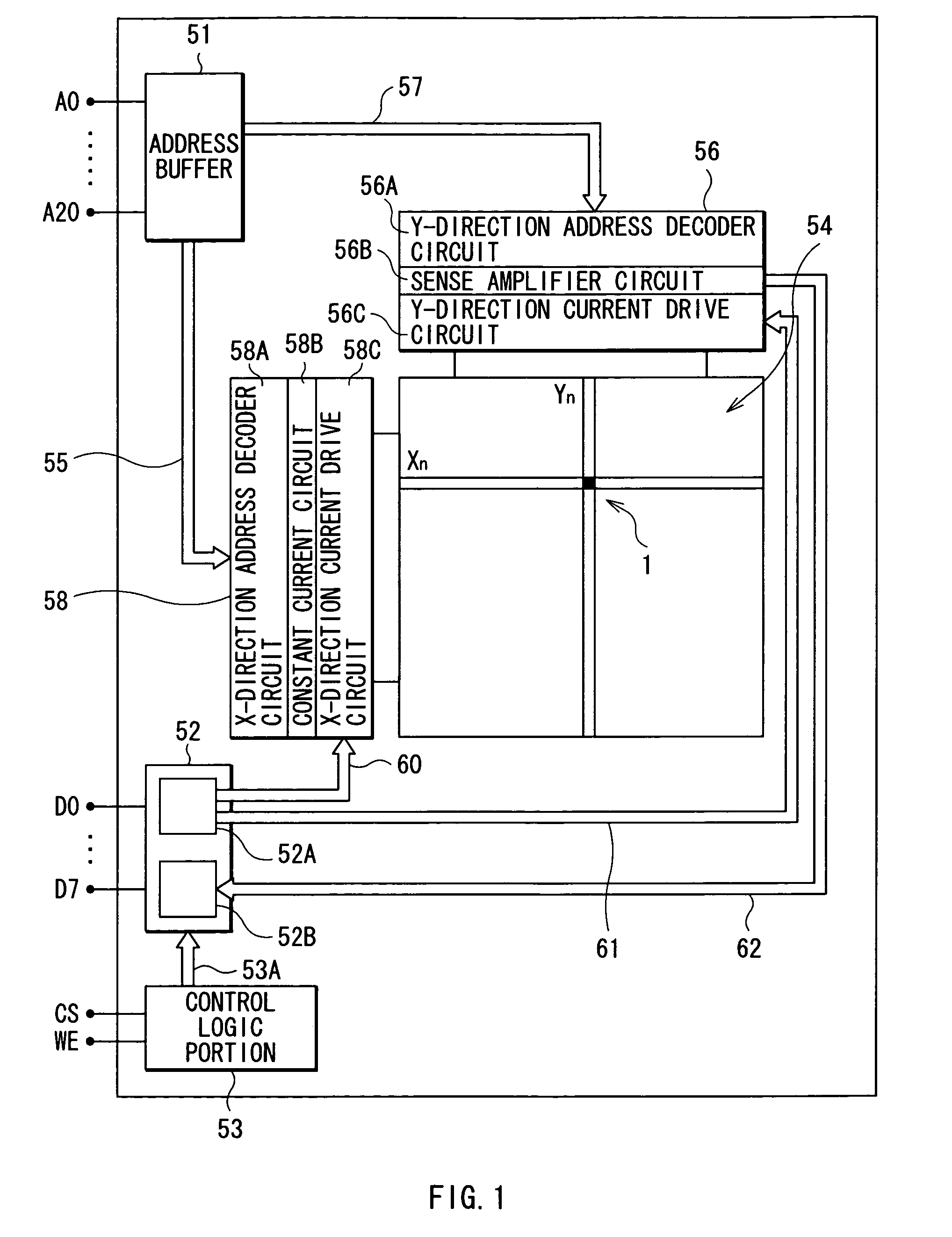
[0086]FIG. 1 is a conceptual diagram showing a general configuration of a magnetic memory device in the embodiment. The magnetic memory device has an address buffer 51, a data buffer 52, a control logic portion 53, a memory cell group 54, a first drive control circuit portion 56, a second drive control circuit portion 58, external address input terminals A0 to A20, and external data terminals D0 to D7.

[0087]The memory cell group 54 has a matrix structure in which a number of memory cells 1 each having a pair of tunneling magnetoresistive devices (hereinbelow, called TMR devices) are arranged in a word line direction (X direction) and a bit line direction (Y direction) which are orthogonal to each other. The memory cell 1 is the minimum unit for storing data in the magnetic memory device and is a concrete example corresponding to ...

second embodiment

[0166]Referring to FIGS. 31 to 35A and 35B, a magnetic memory device of a second embodiment of the invention will now be described.

[0167]FIG. 31 shows a sectional configuration of the memory cell 1H in the magnetic memory device of the embodiment and corresponds to FIG. 5 of the first embodiment. FIG. 32 is an enlarged perspective view of the memory cell 1H and corresponds to FIG. 4. FIG. 33 shows a planar configuration of a magnetic memory device of the modification and corresponds to FIG. 3. In FIGS. 31 to 33, the same reference numerals are designated to the same parts substantially the same as components shown in FIGS. 3 to 5.

[0168]In the following description, the configuration of the magnetic memory device of the second embodiment will be described mainly with respect to the points different from those of the first embodiment, and the other description will be properly omitted.

[0169]In the memory cell 1P of the first embodiment, the write word line 6 and the write bit line 5 a...

third embodiment

[0175]Referring to FIG. 36A, a magnetic memory device of a third embodiment of the invention will now be described.

[0176]FIG. 36A shows a sectional configuration of a memory cell 121P in the magnetic memory device of the embodiment and corresponds to FIG. 5 of the first embodiment. In FIG. 36A, the same reference numerals are designated to the same parts substantially the same as components shown in FIG. 5.

[0177]In the following description, the confignration of the magnetic memory device of the third embodiment and a method of manufacturing the magnetic memory device will be described mainly with respect to the points different from the first embodiment, and the other description will be properly omitted.

[0178]In the memory cell 1 in the magnetic memory device of the first embodiment, the magneto-sensitive layer is constructed by the connection parts 14a and 14b and the second magnetic layers 8a and 8b which are magnetically exchange-coupled to each other. The connection parts 14a ...


PUM


Abstract

The present invention provides a magnetic memory device capable of reducing a loss of a magnetic field generated by currents flowing in a write line and performing writing stably, and a magnetic memory cell mounted on the magnetic memory device. Further, the invention provides a method for easily manufacturing such a magnetic memory device. A magnetic memory cell includes: stacked bodies each including a magneto-sensitive layer whose magnetization direction changes according to an external magnetic field, and constructed so that current flows in a direction perpendicular to a stack layer surface; and a toroidal magnetic layer disposed between the first and second stacked bodies so that the direction along the stack layer surface is set as an axial direction, and constructed so as to be penetrated by a plurality of conductors along the axial direction. Thus, strength reduction in a circulating magnetic field generated in a toroidal magnetic layer can be suppressed, and the magnetization direction of a magneto-sensitive layer in each of the first and second stacked bodies can be inverted by a smaller write current.

Description

TECHNICAL FIELD[0001]The present invention relates to a magnetic memory cell including a magnetoresistive device, a magnetic memory device having a plurality of magnetic memory cells and recording / reading information, and a method of manufacturing the magnetic memory device.BACKGROUND ART[0002]Conventionally, as general memories used for information processors such as a computer and a communication device, volatile memories such as a DRAM (Dynamic Random Access Memory) and an SRAM (Static RAM) are used. The volatile memories have to be refreshed by always supplying current to hold stored information. When the power source is turned off, all of information is lost, so that a nonvolatile memory as means for recording information has to be provided in addition to the volatile memory. For example, a flash EEPROM, a magnetic hard disk drive, or the like is used.[0003]In the nonvolatile memories, as the speed of information processing increases, increase in speed of an access is becoming ...

Claims


Application Information

Patent Timeline
Patent Type & Authority Patents(United States)
IPC IPC(8): G11C11/00G11C11/15H01L21/8246H01L27/10H01L27/105H01L27/22H01L43/08
CPCH01L27/224H01L27/228H01L27/226H10B61/20H10B61/10H10B61/22
Inventor EZAKI, JOICHIROKOGA, KEIJIKAKINUMA, YUJI
Owner TDK CORPARATION
Why Eureka
Try Eureka