

Method for manufacturing a semiconductor device having an alignment feature formed using an N-type dopant and a wet oxidation process
- Summary
- Abstract
- Description
- Claims
- Application Information
AI Technical Summary
Problems solved by technology
Method used
Image

Examples
Embodiment Construction
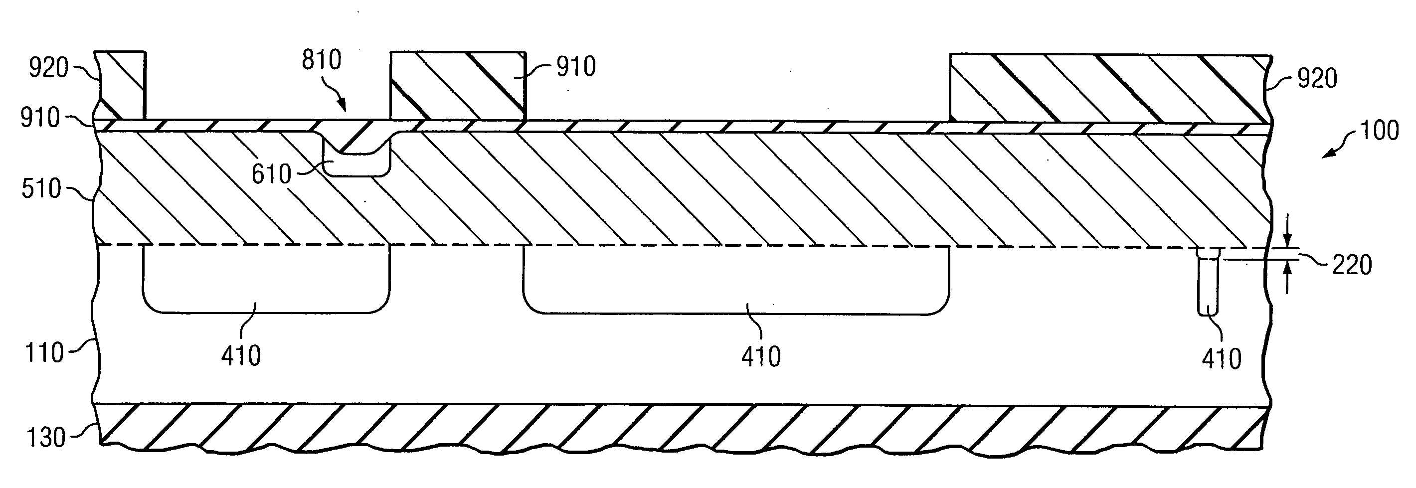
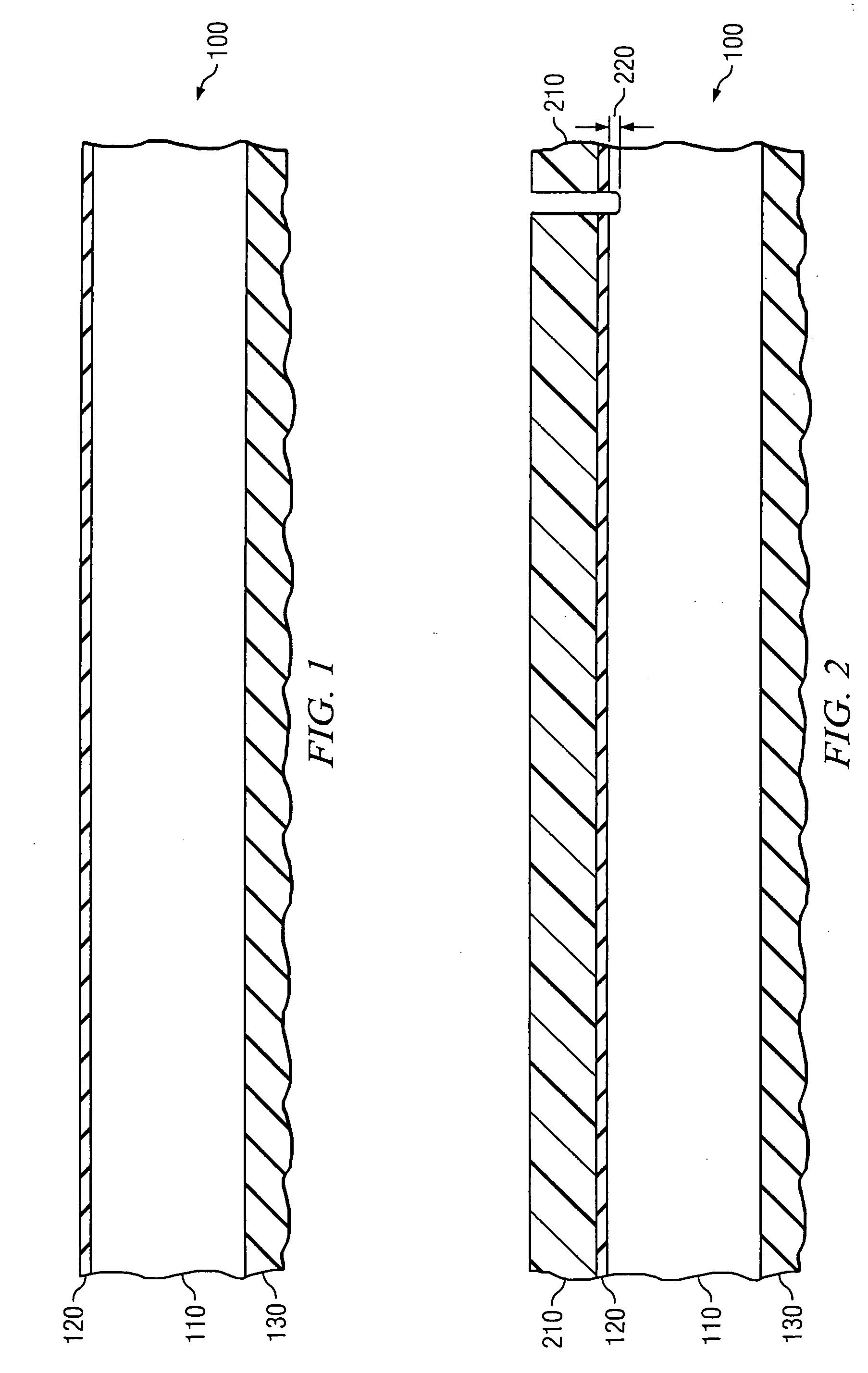
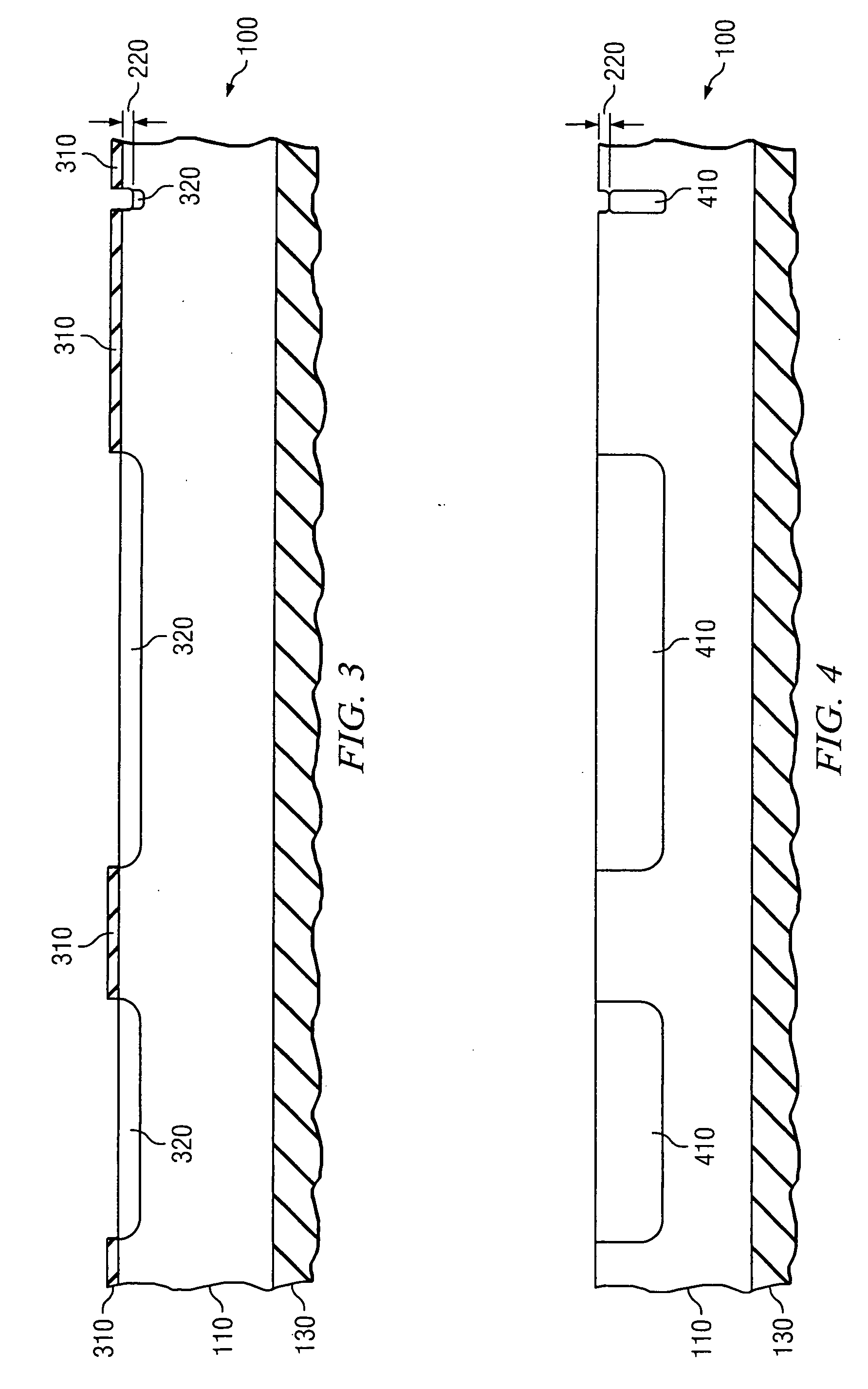
[0022] The present invention is based at least in part on the unique recognition that highly n-type doped substrates, for example silicon substrates, oxidize at a much faster rate than similar substrates having no n-type dopants therein or only small amounts of n-type dopants therein. For example, depending on the amount of n-type dopants within the substrate, the doped substrate oxidizes at a rate of about 2:1 or greater, when compared to an undoped substrate. In an exemplary embodiment, especially when using phosphorous as the dopant and a dose of about 1E15 atoms / cm2 or greater, the doped substrate oxidizes at a rate of about 3:1 compared to an undoped substrate.
[0023] In view of this recognition, the present invention exclusively acknowledged that the n-type dopant could easily and inexpensively be used to precisely form alignment features. As will be discussed more fully with regard to FIGS. 1-12 below, the increased oxidation rate may be used to form a thicker oxide where the...
PUM
 Abstract
Description
Claims
Application Information