Display device and method for manufacturing the same

a technology of display device and substrate, applied in the direction of identification means, instruments, cycles, etc., can solve the problems of reducing brightness, liable to be degraded, and affecting the appearance of display device, so as to reduce the distance between the base substrate and the sealing substrate, and the thickness of the display device can be further decreased.

Inactive Publication Date: 2006-09-14
JOLED INC
View PDF11 Cites 27 Cited by
  • Summary
  • Abstract
  • Description
  • Claims
  • Application Information

AI Technical Summary

Benefits of technology

[0011] Hence, the distance between the sealing substrate and the base substrate depends on the thickness of the masking tape and is set to a value more than the thickness thereof. The masking tape has a relatively large thickness, such as approximately 20 to 40 μm, the distance between the sealing substrate and the base substrate is not decreased smaller than the above thickness, and as a result, a resin material (adhesive) is to be filled into the wide space between the two substrates. This situation prevents further decrease in thickness of display devices.
[0013] Accordingly, it is desirable to have a method for manufacturing a thinner display device, the manufacturing method being capable of sealing organic electroluminescent devices in a resin material provided between a base substrate and a sealing substrate while preventing the spread of the resin material into the terminal electrodes region without a masking tape.
[0017] In the manufacturing method described above, since the second resin material is applied in the region surrounded by the first resin material, the second resin material is prevented from flowing into the region located outside the first resin material, and hence the application of the resin material is restricted in the region surrounded by the first resin material. Hence, the terminal electrodes disposed outside the region surrounded by the first resin material are prevented from being brought into contact with the resin material. Accordingly, it becomes not necessary to cover the terminal electrodes with a masking tape, and as a result, as compared to the case in which a masking tape is used, the distance between the base substrate and the sealing substrate can be decreased.
[0019] According to the embodiments of the present invention described above, since the light-emitting devices may be sealed in the resin material provided between the base substrate and the sealing substrate while the spread of the resin material into the terminal electrodes is prevented without a masking tape, the distance between the base substrate and the sealing substrate can be decreased, and hence the thickness of the display device can be further decreased.

Problems solved by technology

Since having very inferior moisture resistance, the organic electroluminescent device of the display device described above is liable to be degraded by moisture present in the air, and as a result, problems may arise in that areas (dark spots) are generated which do not emit light, the brightness is decreased, and the like.
In manufacturing a display device having the complete solid sealing structure as described above, when an adhesive resin before curing flows and adheres onto terminals (terminal electrodes) for external connection extending from the organic electroluminescent devices, the connection between the display device and an external device with the terminal electrodes provided therebetween becomes unstable.

Method used


Image

  • Display device and method for manufacturing the same
  • Display device and method for manufacturing the same
  • Display device and method for manufacturing the same

Examples


first embodiment

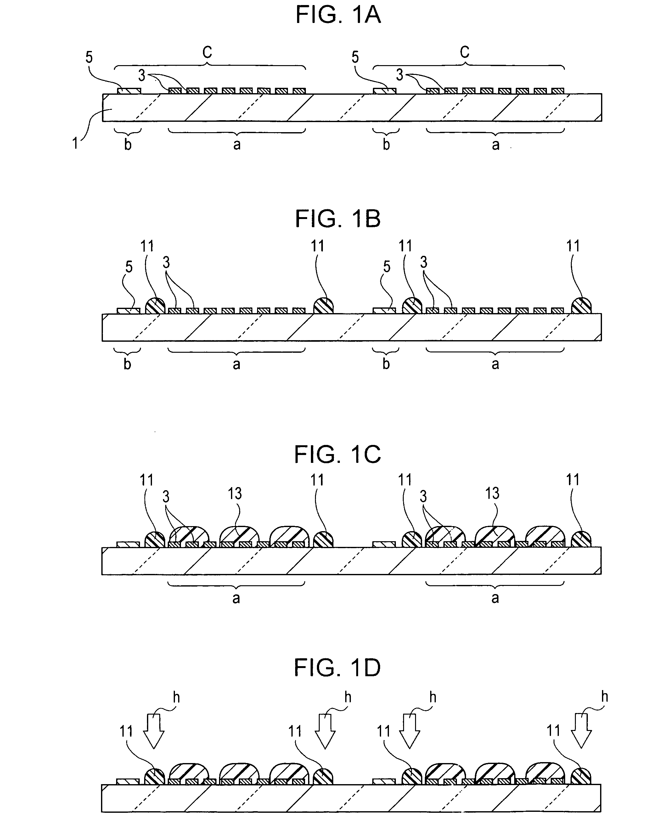
[0026]FIGS. 1A to 1D are each a cross-sectional view of a display device in process for illustrating a manufacturing method according to this embodiment, and the display device is manufactured as described below.

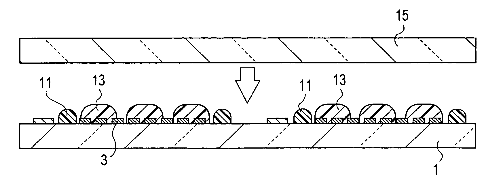
[0027] First, as shown in FIG. 1A, a base substrate 1 is prepared. This base substrate 1 may be formed of a glass material such as a non-alkaline glass and may also be formed, for example, of a plastic material or a film material partly including polycarbonate, polyester, poly(ether sulfone), polyimide, or the like. In addition, on one major surface of the base substrate 1, a plurality of device portions C is provided. In a display region a which is located at the center of each device portion C on the base substrate 1, organic electroluminescent devices 3 are arranged in a matrix, which are connected to respective drive circuits not shown in the figure. In addition, terminal electrodes 5 connected to the respective organic electroluminescent devices 3 are formed in a perip...

second embodiment

[0071]FIGS. 4A to 4D show a method for manufacturing a display device, according to the second embodiment. The difference of the method shown in the figures according to the second embodiment from the above method according to the first embodiment is that the second resin material for sealing the organic electroluminescent devices is formed from a slow-curing resin. The method of this embodiment is performed as described below.

[0072] First, in a step shown in FIG. 4A, as is the case of the first embodiment described with reference to FIG. 1A, the organic electroluminescent devices 3 are formed in an array in the display region a of the base substrate 1, and the terminal electrodes 5 are formed in the peripheral region b.

[0073] Subsequently, as shown in FIG. 4B, a first resin material 21 is formed on the base substrate 1 so as to surround one display region a in which the organic electroluminescent devices 3 are provided and so as to dispose the peripheral region b in which the ter...

third embodiment

[0084]FIGS. 5A to 5D show a method for manufacturing a display device, according to the third embodiment. The difference of the method shown in the figures according to the third embodiment from the above methods according to the first and the second embodiments is that the first resin material and the second resin material are each formed of a slow-curing resin. The method of this embodiment is performed as described below.

[0085] First, in a step shown in FIG. 5A, as is the case of the first embodiment described with reference to FIG. 1A, the organic electroluminescent devices 3 are formed in an array in the display region a of the base substrate 1, and the terminal electrodes 5 are formed in the peripheral region b.

[0086] Next, as shown in FIG. 5B, the first resin material 11 composed of a slow-curing resin similar to that in the first embodiment is formed on the base substrate 1 so as to surround one display region a in which the organic electroluminescent devices 3 are provide...


PUM

PropertyMeasurementUnit
thicknessaaaaaaaaaa
thicknessaaaaaaaaaa
volume ratioaaaaaaaaaa

Abstract

A method for manufacturing a display device and a display device manufactured thereby are provided. The above method has the steps of forming a first resin material on a base substrate so as to surround a region in which light-emitting devices are provided, applying a second resin material in the region surrounded by the first resin material, initiating polymerization of at least one of the above resin materials, adhering the base substrate to the sealing substrate with the above two resin materials provided therebetween after the polymerization is initiated so as to seal the light-emitting devices in the second resin material, and curing the first resin material and the second resin material by promoting the polymerization.

Description

CROSS REFERENCES TO RELATED APPLICATIONS [0001] The present invention contains subject matter related to Japanese Patent Application JP 2005-048224 filed in the Japanese Patent Office on Feb. 24, 2005, the entire contents of which are incorporated herein by reference.BACKGROUND OF THE INVENTION [0002] 1. Field of the Invention [0003] The present invention relates to display devices, and more particularly, relates to a display device including a substrate provided with light-emitting devices and a sealing substrate which is adhered to the substrate and to a method for manufacturing the display device. [0004] 2. Description of the Related Art [0005] As a next-generation display device, a display device using organic electroluminescent devices has drawn attention. This display device has the following various features: the viewing angle is wide since self-luminous organic electroluminescent devices are used, energy saving may be obtained since a backlight is not necessary, the responsi...

Claims


Application Information

Patent Timeline
Patent Type & Authority Applications(United States)
IPC IPC(8): H01L33/00G09F9/30H01L27/32H01L51/50H05B33/04H05B33/10
CPCH01L51/5237H01L51/56H01L2251/566H10K50/8426H10K71/851H10K71/00B62K17/00B62K5/02B62K3/002
Inventor HAYASHI, NAOKI
Owner JOLED INC
Why Eureka
Try Eureka