Radio-frequency module for communication and method of manufacturing the same

a radio frequency module and communication technology, applied in the field of radio frequency modules for communication, can solve the problems of high production cost, inability to lower the module production cost, and delay in the development and actual use of electronic devices that utilize electric waves in milliwave bands. , to achieve the effect of reducing material cost and cost, reducing production cost, and easy increase of through hole accuracy

Inactive Publication Date: 2006-09-14
FUJITSU LTD
View PDF4 Cites 47 Cited by
  • Summary
  • Abstract
  • Description
  • Claims
  • Application Information

AI Technical Summary

Benefits of technology

[0014] In accordance with the present invention, the supporting body core member of the supporting body is made of a resin material. Accordingly, the through hole to form the waveguide in the supporting body can be formed at a much lower cost than in a case where such a through hole is formed in a ceramic substrate or a metal substrate. Also, the accuracy of processing the through hole can be readily increased.
[0015] In accordance with the present invention, the semiconductor device and the antenna element are disposed on the opposite sides of the supporting body, and the waveguide penetrating the supporting body is formed so as to integrate the semiconductor device and the antenna element. Also, the supporting body core member of the supporting body is made of a resin material, so as to lower the material costs and the cost for processing the through hole to form the waveguide. Thus, a low-cost communication radio-frequency module and a method of manufacturing the communication radio-frequency module can be provided.

Problems solved by technology

Particularly, electric waves in milliwave bands involving broad frequency bands that have not been used yet are suitable for high-speed, large-capacity information transmission that requires broad frequency bandwidths.
Despite the high possibility of practical use, there are delays in the development and actual use of electronic apparatuses that utilize electric waves in milliwave bands, because of the high production costs of measurement instruments for millimeter electric waves and milliwave-band communication semiconductor devices that are required for the development of such electronic apparatuses.
However, the module 100 illustrated in FIG. 1 has the problem of high production costs.
As a result, the hermitically sealed package 106 has the problem of being not able to lower the module production costs.
However, it is difficult to form a highly precise opening in the ceramic board 111, and doing so only increases the processing cost.
In a case where a metal board is used instead of the ceramic board 111, the material cost for the metal board is low, but the transmission characteristics deteriorate, because a highly precise opening cannot be formed by press stamping.
To do so, however, the processing cost increases, and the module production costs cannot be lowered.

Method used


Image

  • Radio-frequency module for communication and method of manufacturing the same
  • Radio-frequency module for communication and method of manufacturing the same
  • Radio-frequency module for communication and method of manufacturing the same

Examples


first embodiment

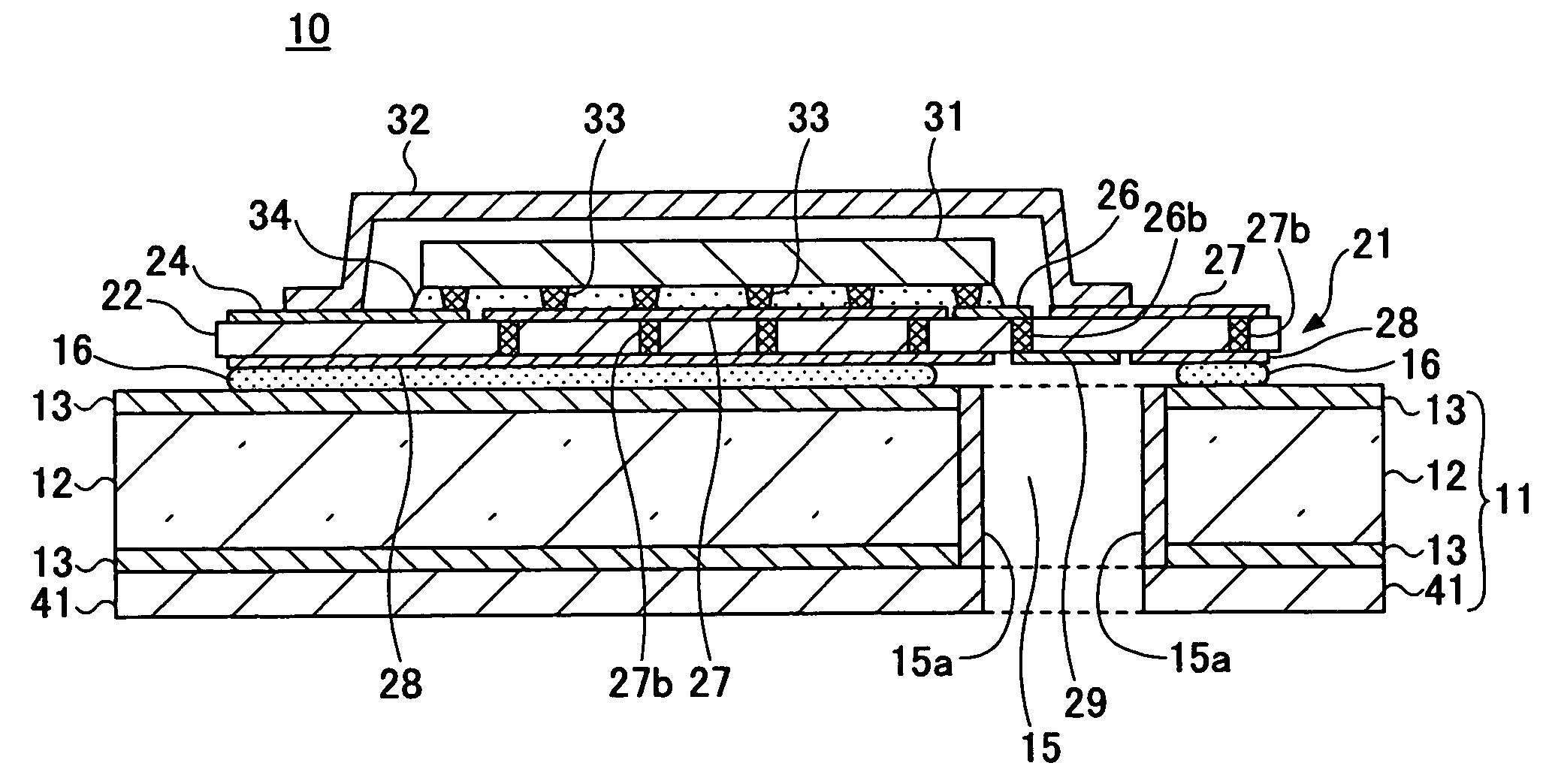
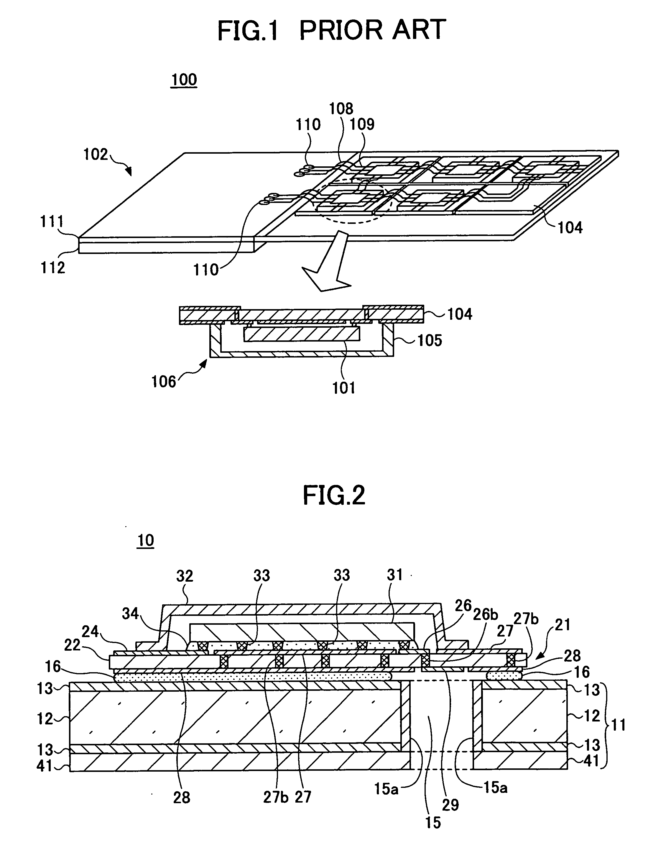
[0028]FIG. 2 is a cross-sectional view of a radio-frequency module for communication in accordance with a first embodiment of the present invention.

[0029] As shown in FIG. 2, the communication radio-frequency module 10 of this embodiment includes: a supporting body 11 in which a waveguide 15 is formed; a wiring board 21 that is fixed onto the supporting body 11; a semiconductor device 31 that is flip-chip mounted on the wiring board 21; a cap 32 that covers the semiconductor device 31; and an antenna element 41 that is fixed to the bottom surface of the supporting body 11.

[0030] The semiconductor device 31 may be formed with an MMIC (monolithic microwave IC), for example. Although not shown, the MMIC includes: a semiconductor substrate that has an active element such as an FET (field-effect transistor) and is made of GaAs or Si; a resistive element that is formed on the insulating layer on the surface of the semiconductor substrate; and a circuit pattern to which a passive element...

second embodiment

[0068]FIG. 7 is a schematic cross-sectional view of a communication radio-frequency module in accordance with a second embodiment of the present invention. In this drawing, the same components as those of the first embodiment are denoted by the same reference numerals as those in the first embodiment, and explanation of them is omitted in the following description.

[0069] As shown in FIG. 7, the communication radio-frequency module 60 is the same as the communication radio-frequency module 10 in accordance with the first embodiment, except that a ceramic film 62 is interposed between the supporting body core member 12 and the conductive film 13 on the upper surface side of a supporting body 61 (on the side of the wiring board 21).

[0070] The ceramic film 62 may be made of alumina, crystallize glass, aluminum nitride of 500 μm in thickness, or a mixed material of those materials, for example. The ceramic film 62 is fixed to the supporting body core member 12 with an adhesive agent. T...


PUM


Abstract

A communication radio-frequency module is provided that has a semiconductor device to which an antenna element is connected. This communication radio-frequency module includes: a supporting body that has a waveguide formed therein; a wiring board that is fixed onto a surface of the supporting body; the semiconductor device that is flip-chip mounted onto the wiring board by ultrasonic bonding; and the antenna element that is disposed on the other surface of the supporting body. In this module, the wiring board includes a board core member that is made of a resin material, and the supporting body includes a supporting body core member that is also made of a resin material.

Description

CROSS-REFERENCE TO RELATED APPLICATION [0001] This patent application is based upon and claims the benefit of priority from Japanese Patent Application No. 2005-066027, filed on Mar. 9, 2005, the entire contents of which are hereby incorporated by reference. BACKGROUND OF THE INVENTION [0002] The present invention generally relates to radio-frequency modules for communication, and, more particularly, to a radio-frequency module that is equipped with an antenna device and is designed for communication in microwave bands or milliwave bands, and a method of manufacturing the radio-frequency module. [0003] In recent years, electronic apparatuses that utilize electric waves in microwave bands or milliwave bands have been increasingly produced. Particularly, electric waves in milliwave bands involving broad frequency bands that have not been used yet are suitable for high-speed, large-capacity information transmission that requires broad frequency bandwidths. Having features such as high-...

Claims


Application Information

Patent Timeline
Patent Type & Authority Applications(United States)
IPC IPC(8): H01L29/40H01Q9/04
CPCH01L2924/16152H01Q1/22H01L2924/15192H01L2224/73204H01L2224/32225H01Q1/2283H01Q9/04H01Q9/0407H01Q21/0025H05K1/0237H05K3/0058H01L2224/16225H01L2924/00H01L2924/00014H01L2924/00011H01L2224/0401
Inventor IIJIMA, SHINYAABE, TOMOYUKIHAYASHI, NOBUYUKIOHASHI, YOJISHIMURA, TOSHIHIRO
Owner FUJITSU LTD
Why Eureka
Try Eureka