DRAM with high K dielectric storage capacitor and method of making the same

a dielectric storage capacitor and high k dielectric technology, applied in the field of dielectric storage capacitors with high k dielectric storage capacitors and a method of making the same, can solve the problem of slow leakage of capacitor charge, and achieve the effect of minimizing the interfacial contribution to eo

Inactive Publication Date: 2006-09-14
GOVINDARAJAN SHRINIVAS
View PDF60 Cites 29 Cited by
  • Summary
  • Abstract
  • Description
  • Claims
  • Application Information

AI Technical Summary

Benefits of technology

[0012] Metals, such as titanium, form a solid solution with oxygen and are, therefore, very effective as gettering layers. Furthermore, formation of a conductive silicide layer at the interface would be very useful for creating MIM capacitors. Alternatively, if processing conditions are selected such that a silicate layer forms, the uniformity and higher dielectric constant of such a layer would help to minimize the interfacial contribution to EOT. The segregation of oxygen can be tailored (through temperature, time, and partial pressure control) such that a pure silicide is in contact with the silicon substrate and the silicate / oxide is formed above the silicide layer.
[0013] The high K layer is based on TiO2, which has a dielectric constant in the range of 80. However, TiO2 by itself will not be adequate due to the low band gap (˜3.05 eV) and the negligible conduction band offset to Si (close to 0 eV). Combining TiO2 with higher band gap materials (even though they may have lower dielectric constant) is one possibility. Some possibilities include HfO2, Ta2O5, SrO (dielectric constant for SrTiO3 is close to 100) and certain dielectric nitrides (e.g., Hf3N4, ZrN4). The two broad categories of dielectrics proposed here are either mixed oxides / nitrides based on Ti and Ta (Hf—Ti—Ta—O—N) or nanolaminates of the same (using combinations or subsets of TiO2, HfO2, Hf3N4, Ta2O5 . . . ). The mixed films are deposited by ALD of the individual components (e.g. HfO2 using TEMAHf and O3 or H2O, TiO2 using either TiCl4 or Ti(OEt)4 and O3 or H2O, Ta2O5 using TBTEMT and O3 or H2O, Hf3N4 using TEMAHf with NH3, etc.) with the thickness of each layer adjusted to ensure intimate film mixing. The nanolaminate structures are formed by using thicker sub-layers of each component film. The nanolaminate structures provide a key benefit in terms of preventing grain growth and controlling the crystallization behavior of the dielectric film.

Problems solved by technology

In any practical device, charge will slowly leak from the capacitor.
A key challenge is to optimize the various interface properties and to use dielectrics with high capacitance.

Method used


Image

  • DRAM with high K dielectric storage capacitor and method of making the same
  • DRAM with high K dielectric storage capacitor and method of making the same
  • DRAM with high K dielectric storage capacitor and method of making the same

Examples


Embodiment Construction

[0020] The making and using of the presently preferred embodiments are discussed in detail below. It should be appreciated, however, that the present invention provides many applicable inventive concepts that can be embodied in a wide variety of specific contexts. The specific embodiments discussed are merely illustrative of specific ways to make and use the invention, and do not limit the scope of the invention.

[0021] The present invention will be described with respect to preferred embodiments in a specific context, namely a DRAM cell. The invention may also be applied, however, to other devices that include capacitors. For example, any integrated circuit that uses a capacitor can benefit from the teachings of the present invention.

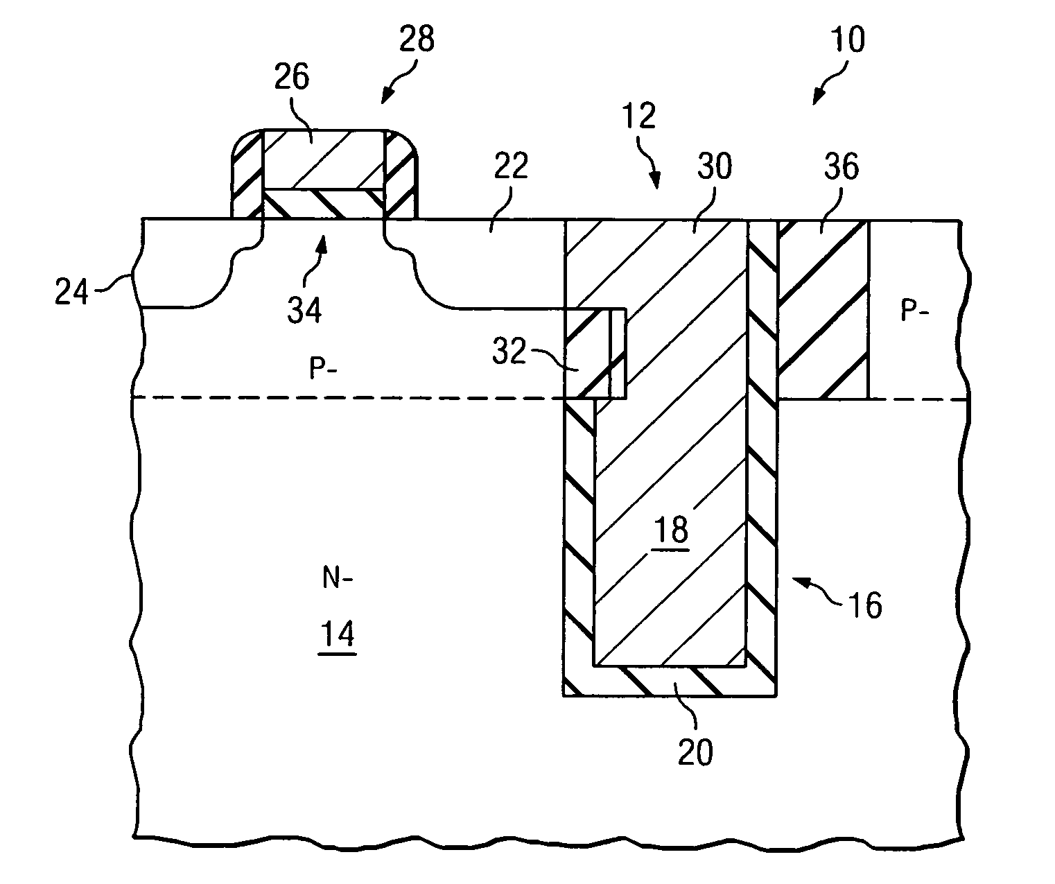
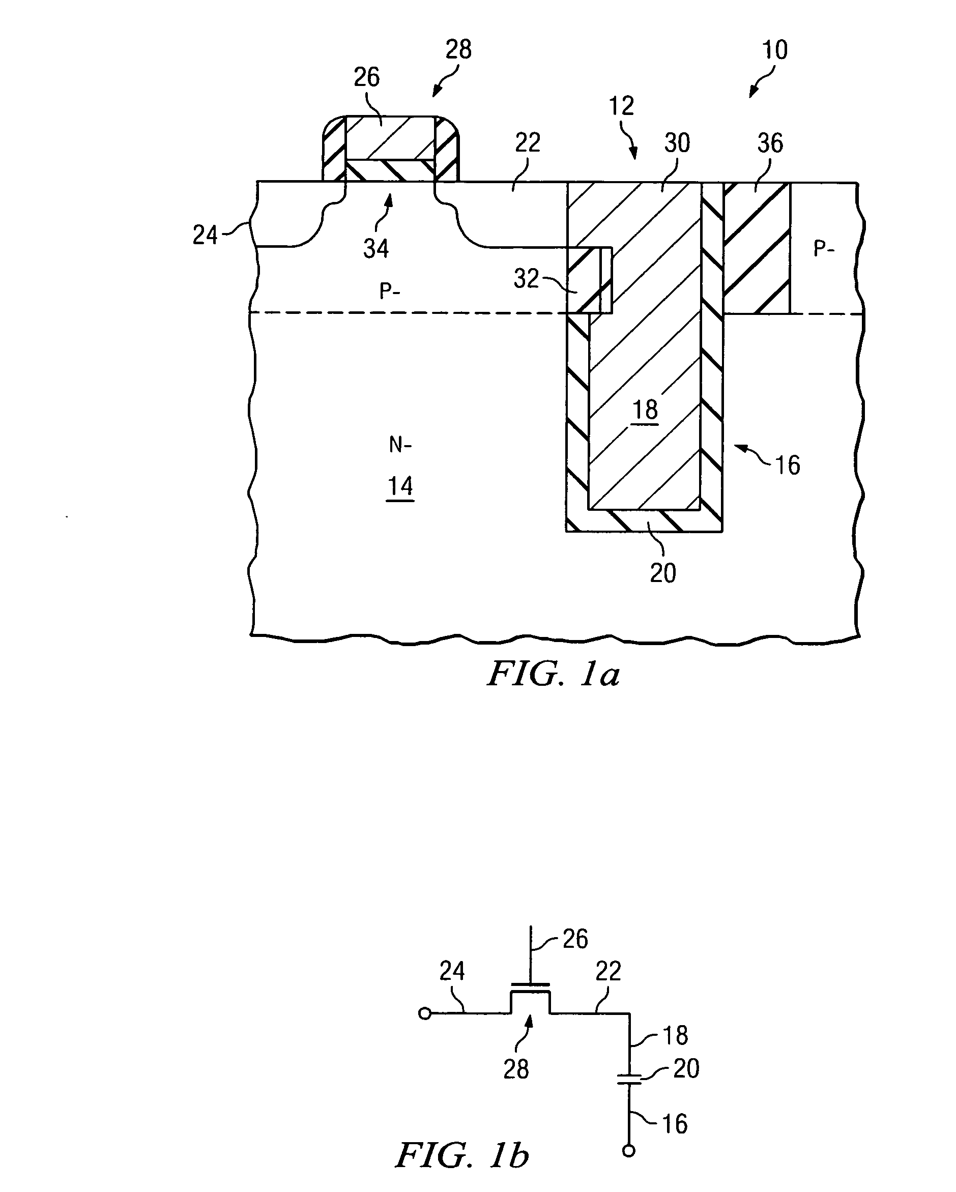
[0022]FIG. 1a shows a first example of a DRAM cell 10 that can utilize concepts of the present invention. FIG. 1b shows a schematic diagram of the cell of FIG. 1a. The embodiment of FIG. 1a includes a trench capacitor 12, which is formed in the semico...


PUM

PropertyMeasurementUnit
melting pointaaaaaaaaaa
dielectric constantaaaaaaaaaa

Abstract

A memory cell is fabricated by forming a first capacitor electrode including silicon. A metal layer is formed in physical contact with the first capacitor electrode. The metal layer is formed from a material having a high affinity for oxygen and a melting point above about 1000° C. A layer of high K dielectric material is formed in physical contact with the metal layer. The high K dielectric material has a dielectric constant greater than about 5. A conductive layer is formed over the high K dielectric material layer. An interface between the high K dielectric layer and the metal layer / silicon body is modified by performing an annealing step. A transistor is also formed to be electrically coupled to one of the conductive layer or the first capacitor electrode.

Description

[0001] This application is a divisional of co-pending application Ser. No. 11 / 031,691, entitled “DRAM with High K Dielectric Storage Capacitor and Method of Making the Same,” filed Jan. 7, 2005, which application is incorporated herein by reference. CROSS-REFERENCE TO RELATED APPLICATIONS [0002] This application is related to the following co-pending applications, both of which are incorporated herein by reference: application Ser. No. 11 / 031,716, filed Jan. 7, 2005, and entitled “High Dielectric Constant Materials” (Attorney Docket 2004P54456) and application Ser. No. 11 / 031,596, filed Jan. 7, 2005, and entitled “Method to Control Interfacial Properties for Capacitors Using a Metal Layer” (Attorney Docket 2004P54458).TECHNICAL FIELD [0003] The present invention relates generally to semiconductor devices and methods, and more particularly to a DRAM with a high K dielectric storage capacitor and a method of making the same. BACKGROUND [0004] A dynamic random access memory (DRAM) is a...

Claims


Application Information

Patent Timeline
Patent Type & Authority Applications(United States)
IPC IPC(8): H01L21/8242
CPCH01L27/1087H01L29/945H10B12/0387
Inventor GOVINDARAJAN, SHRINIVAS
Owner GOVINDARAJAN SHRINIVAS
Why Eureka
Try Eureka