Floating body germanium phototransistor

a phototransistor and floating body technology, applied in the field of integrated circuit (ic) fabrication, can solve the problems of imperfect bottom interface between ge single crystal and bottom dielectric layer (si/sub>3/sub>n/sub>4), leakage current in diodes, and deterioration of electrical performance at the bottom interface, so as to minimize the contribution of imperfect bottom interface to the electrical characteristics of the devi

Active Publication Date: 2007-01-04
SHARP KK AKA SHARP CORP +1
View PDF1 Cites 6 Cited by
  • Summary
  • Abstract
  • Description
  • Claims
  • Application Information

AI Technical Summary

Benefits of technology

[0008] The present invention describes a method for fabricating a floating body Ge MOS transistor for infrared (IR) photo detection. The floating body Ge MOS transistor minimizes the contribution of the imperfect bottom interface to the device's electrical characteristics.

Problems solved by technology

However, it is noted that the interface between Ge single crystal and the bottom dielectric layer (Si3N4) is not perfect, as shown in the TEM image.
This interface may potentially cause leakage current in the diode.
This interface is likely the result of the Ge PIN diode using the entire Ge film, so that the bottom interface deteriorates the electrical performance.

Method used


Image

  • Floating body germanium phototransistor
  • Floating body germanium phototransistor
  • Floating body germanium phototransistor

Examples


Embodiment Construction

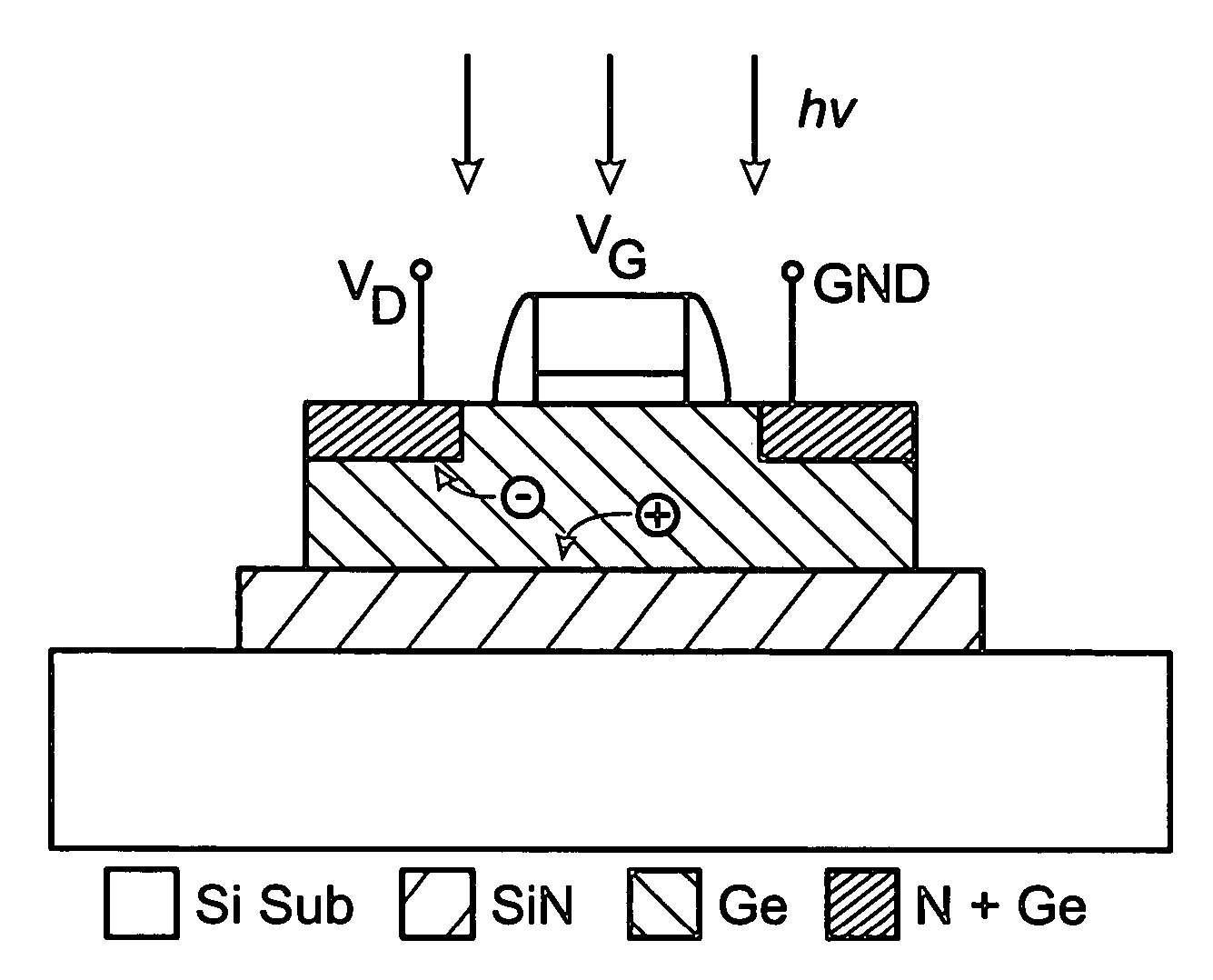
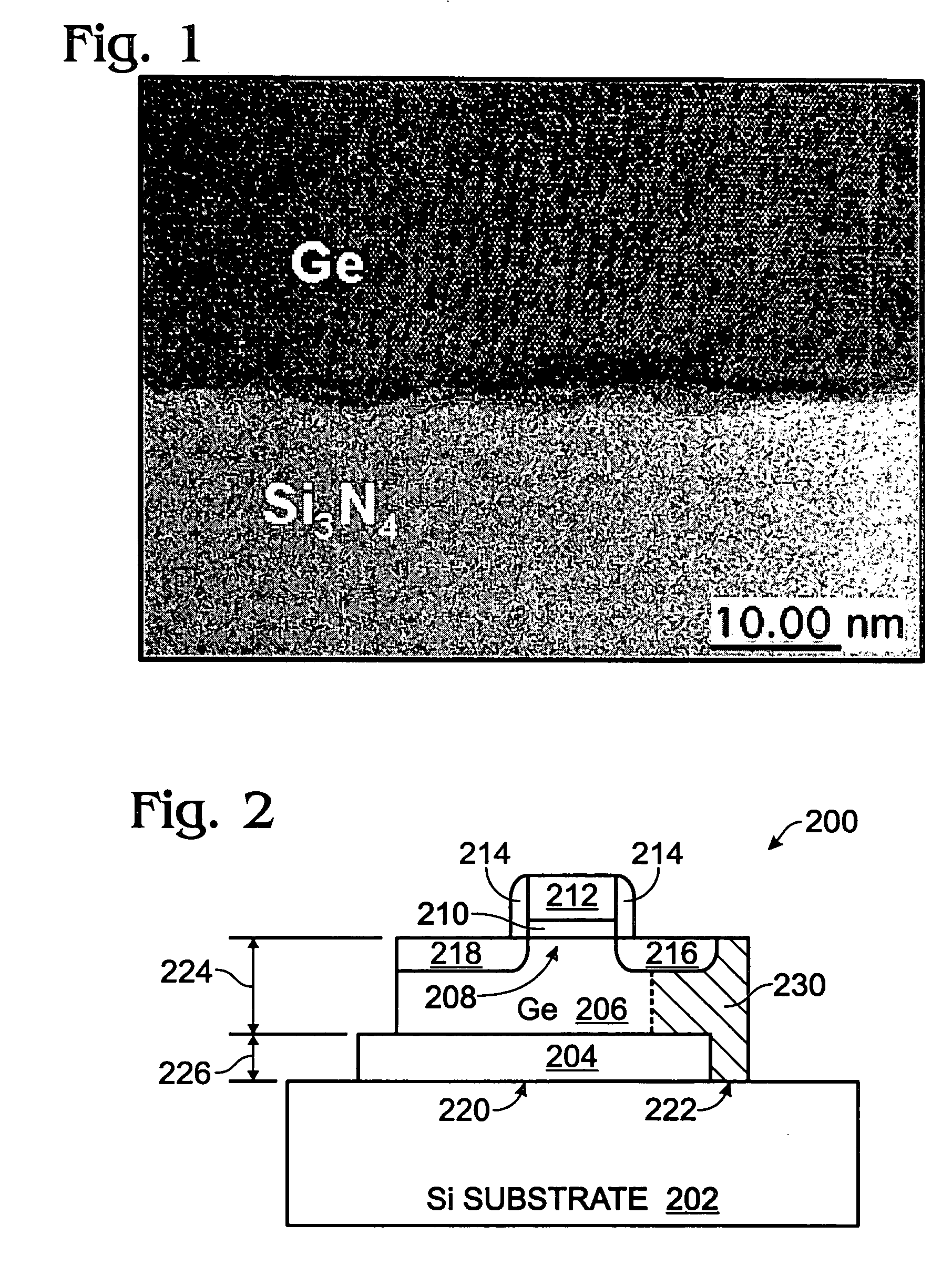
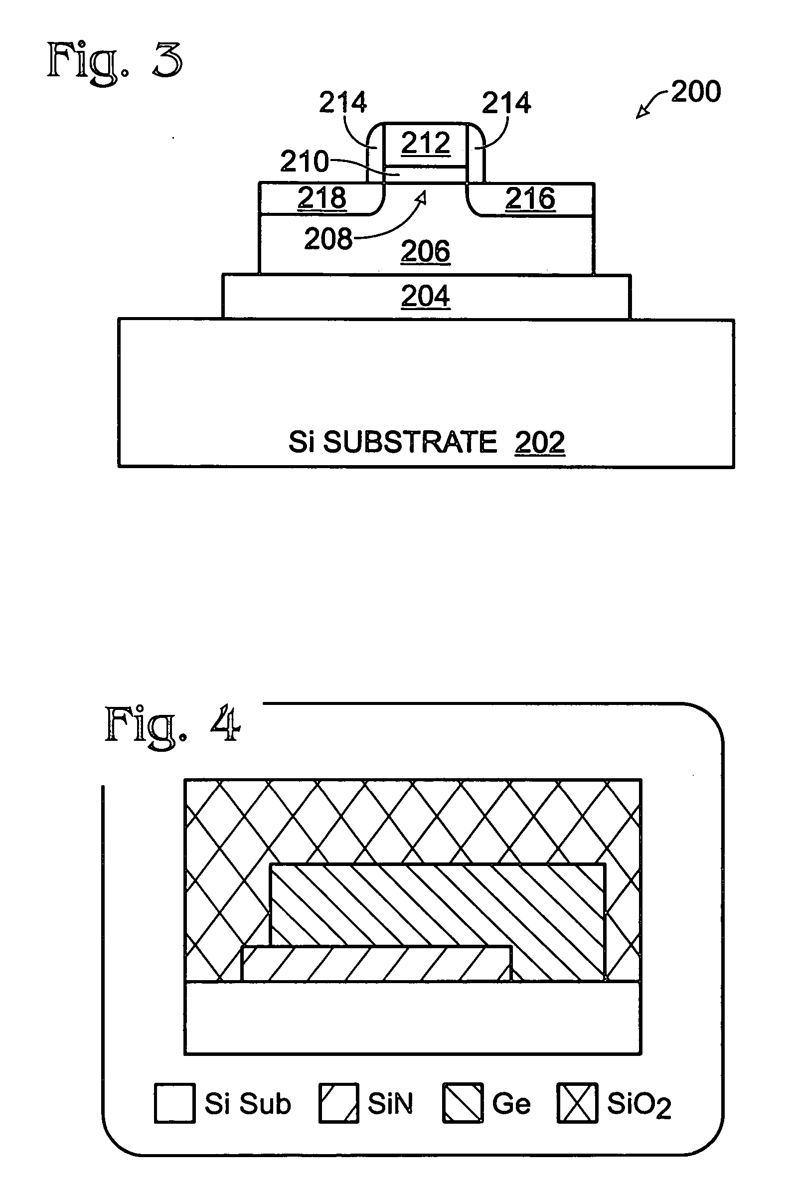
[0021]FIG. 2 is a partial cross-sectional view of a floating body germanium (Ge) phototransistor. The phototransistor 200 comprises a silicon (Si) substrate 202 and an insulator layer 204 overlying the Si substrate 202. An epitaxial Ge layer 206 overlies the insulator layer 204. A channel region 208 is formed in the Ge layer 206. A gate dielectric 210, gate electrode 212, and gate spacers 214 overlie the channel region 208. A source 216 and a drain 218 are formed in the Ge layer 206.

[0022] More specifically, the insulator layer 204 overlies a first surface 220 of the Si substrate 202, exposing a second surface 222 of the Si substrate. The epitaxial Ge layer 206 is formed overlying the insulator layer 204 and the Si substrate second surface 222. Typically, the epitaxial Ge layer 206 has a thickness 224 (above the insulator 204) in the range of 20 to 1000 nm. The insulator layer 204 typically has a thickness 226 in the range of 10 to 500 nanometers (nm).

[0023] In one aspect, the gat...


PUM


Abstract

A floating body germanium (Ge) phototransistor and associated fabrication process are presented. The method includes: providing a silicon (Si) substrate; selectively forming an insulator layer overlying the Si substrate; forming an epitaxial Ge layer overlying the insulator layer using a liquid phase epitaxy (LPE) process; forming a channel region in the Ge layer; forming a gate dielectric, gate electrode, and gate spacers overlying the channel region; and, forming source/drain regions in the Ge layer. The LPE process involves encapsulating the Ge with materials having a melting temperature greater than a first temperature, and melting the Ge using a temperature lower than the first temperature. The LPE process includes: forming a dielectric layer overlying deposited Ge; melting the Ge; and, in response to cooling the Ge, laterally propagating an epitaxial growth front into the Ge from an underlying Si substrate surface.

Description

BACKGROUND OF THE INVENTION [0001] 1. Field of the Invention [0002] This invention generally relates to integrated circuit (IC) fabrication and, more particularly, to a germanium (Ge) phototransistor and associated fabrication process that capitalizes on the floating body effect of a device insulated from an underlying substrate. [0003] 2. Description of the Related Art [0004]FIG. 1 is a Cross-Sectional Transmission Electron Microscopy (XTEM) image of an interface between Ge and Si3N4. The Ge film has been regrown by liquid phase epitaxy. In a co-pending application entitled METHOD OF EPITAXIAL GROWTH OF GERMANIUM PHOTODETECTOR FOR CMOS IMAGER, Lee et al., Ser. No. 11 / 069,424, filed Feb. 28, 2005, a method for growing single crystalline Ge film by liquid phase epitaxy is presented, along with a means of fabricating a PIN photo detector for infrared photon detection. However, it is noted that the interface between Ge single crystal and the bottom dielectric layer (Si3N4) is not perfe...

Claims


Application Information

Patent Timeline
Patent Type & Authority Applications(United States)
IPC IPC(8): H01L31/00
CPCH01L31/028Y02E10/547H01L31/1808H01L31/1136
Inventor LEE, JONG-JANHSU, SHENG TENGMAA, JER-SHENTWEET, DOUGLAS J.
Owner SHARP KK AKA SHARP CORP
Why Eureka
Try Eureka