

Bonding pads having slotted metal pad and meshed via pattern
a bonding pad and slotted metal technology, applied in semiconductor devices, solid-state devices, printed circuit details, etc., can solve problems such as undesirable thinning of materials, process for producing such structures, and resistance to certain limitations and problems, and achieve the effect of reducing vertical overlap
- Summary
- Abstract
- Description
- Claims
- Application Information
AI Technical Summary
Benefits of technology
Problems solved by technology
Method used
Image

Examples
Embodiment Construction
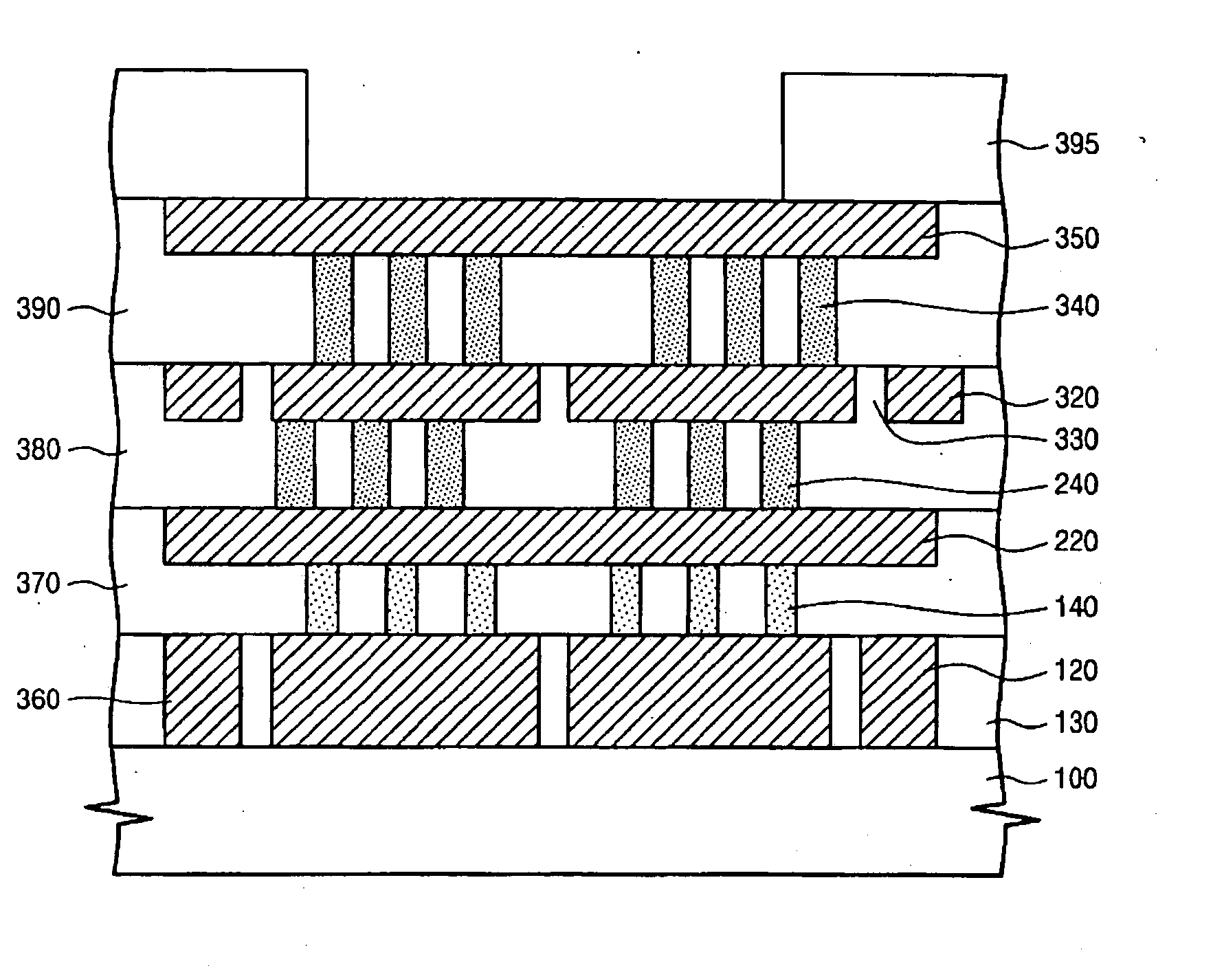
[0042] The present invention provides a range of bonding pad structures that incorporate via patterns and slotted metal pads and methods of fabricating such structures for addressing the deficiencies of the conventional bonding pad constructions.
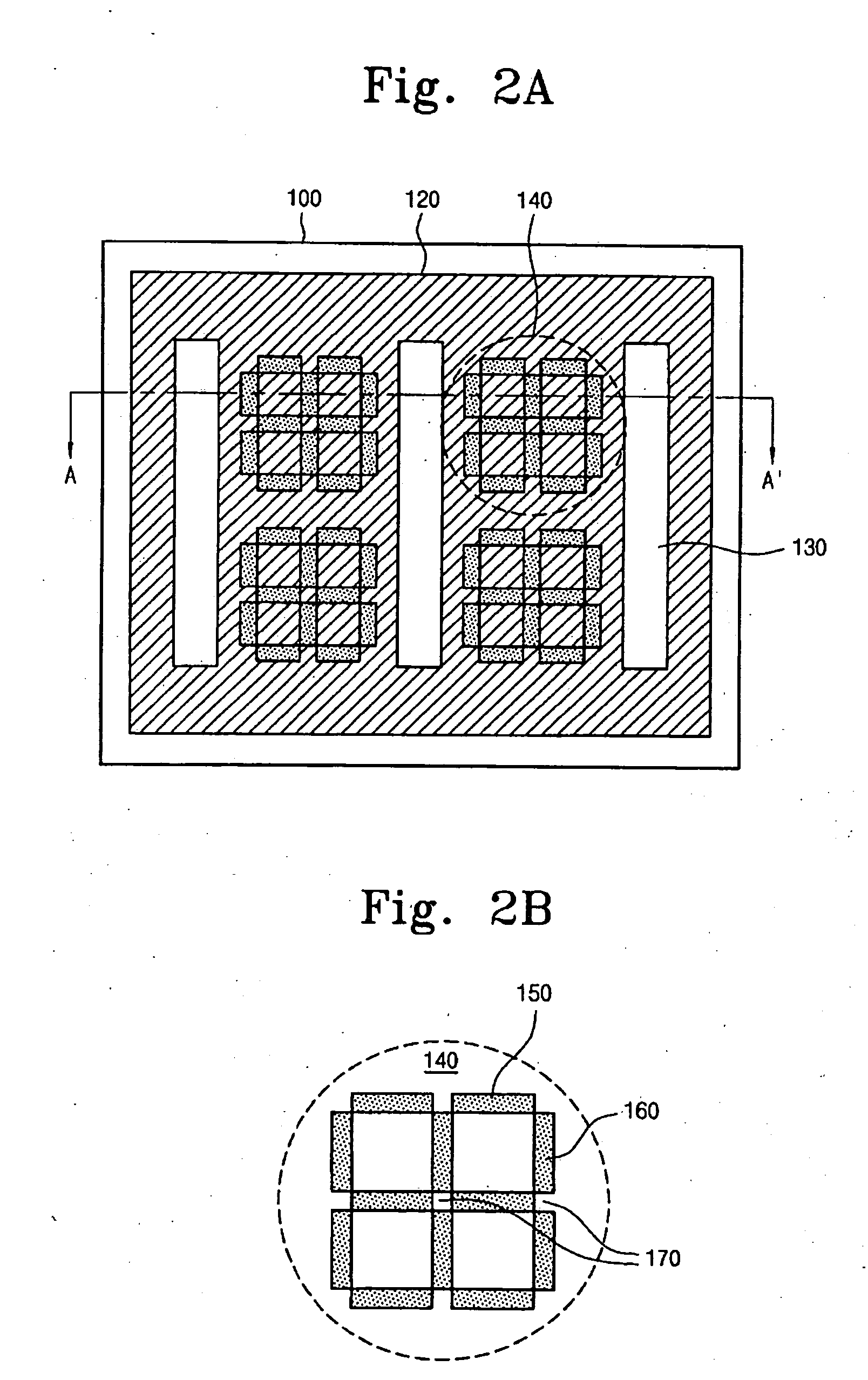
[0043] As illustrated in FIG. 2A, a metal pad 120 is formed on a substrate 100. The metal pad includes at least one slot 130, e.g., an elongated opening formed at least partially through the metal layer from which the metal pad is formed, and a first interlayer dielectric is formed over the first (or Nth) metal pad. Although as illustrated the opening formed in the metal pad120 is an elongated slot 130, those skilled in the art will appreciate that the opening may be readily adapted to provide a wide range of configurations of dielectric regions exposed within the periphery of the metal pad.
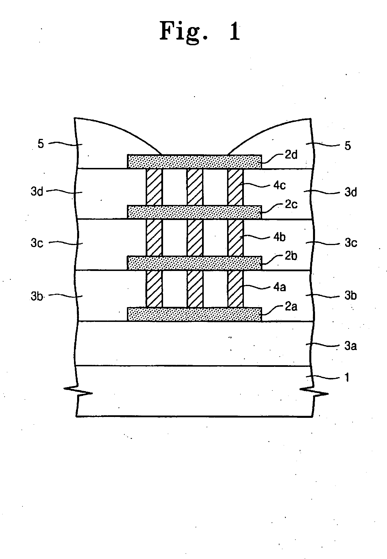
[0044] As used herein, N and Nth are to be considered interchangeable variables which refer to a level or a structure arranged below, i.e., formed earl...
PUM
 Abstract
Description
Claims
Application Information