A Method for the Manufacture of a Piezoelectric Element

a piezoelectric element and manufacturing method technology, applied in the direction of variable capacitors, generators/motors, conductive pattern formation, etc., can solve the problems of poor piezoelectric characteristics, insufficient printing performance of ink-jet recording heads or printers, and difficult to obtain piezoelectric films with prescribed orientation degrees with etc., to achieve stable and good piezoelectric characteristics, good stability and reproducibility, excellent characteristics

Inactive Publication Date: 2006-09-21
SEIKO EPSON CORP
View PDF20 Cites 13 Cited by
  • Summary
  • Abstract
  • Description
  • Claims
  • Application Information

AI Technical Summary

Benefits of technology

[0008] Accordingly, it is an object of the present invention to provide a piezoelectric element with stable and good piezoelectric characteristic by obtaining the prescribed orientation degree of piezoelectric film with good stability and reproducibility and also a method for the manufacture of such a piezoelectric element. Another object of the present invention is to provide a piezoelectric element demonstrating excellent characteristics by improving the uniformity of the bottom electrode thickness and eliminating the discontinuity of crystals of the piezoelectric film and also a method for the manufacture of such a piezoelectric element.
[0011] Forming a piezoelectric film in two stages makes it possible to form PZT having stable 100 plane orientation degree which is not affected by humidity or the like. Furthermore, the non-uniformity of the bottom electrode thickness and discontinuity of piezoelectric crystals can be prevented.
[0013] Forming a Ti layer in two stages makes it possible to form a piezoelectric film having a stable 100 plane orientation degree which is not affected by humidity or the like.

Problems solved by technology

However, the problem associated with the conventional piezoelectric elements was that piezoelectric films with prescribed orientation degree were difficult to obtain with good stability and reproducibility.
Such piezoelectric elements could not provide stable and good piezoelectric characteristics and accounted for insufficient printing performance of ink-jet recording heads or printers.
The prescribed orientation degree of piezoelectric film was especially difficult to obtain with good stability and reproducibility when a bottom electrode formed on a diaphragm was patterned to the prescribed shape and then a piezoelectric film was formed on the bottom electrode.
Another problem was that the thickness of the bottom electrode became non-uniform and the crystals of the piezoelectric film became discontinuous in the vicinity of the patterning boundary of bottom electrode.

Method used


Image

  • A Method for the Manufacture of a Piezoelectric Element
  • A Method for the Manufacture of a Piezoelectric Element
  • A Method for the Manufacture of a Piezoelectric Element

Examples


first embodiment

Manufacturing Method of the First Embodiment

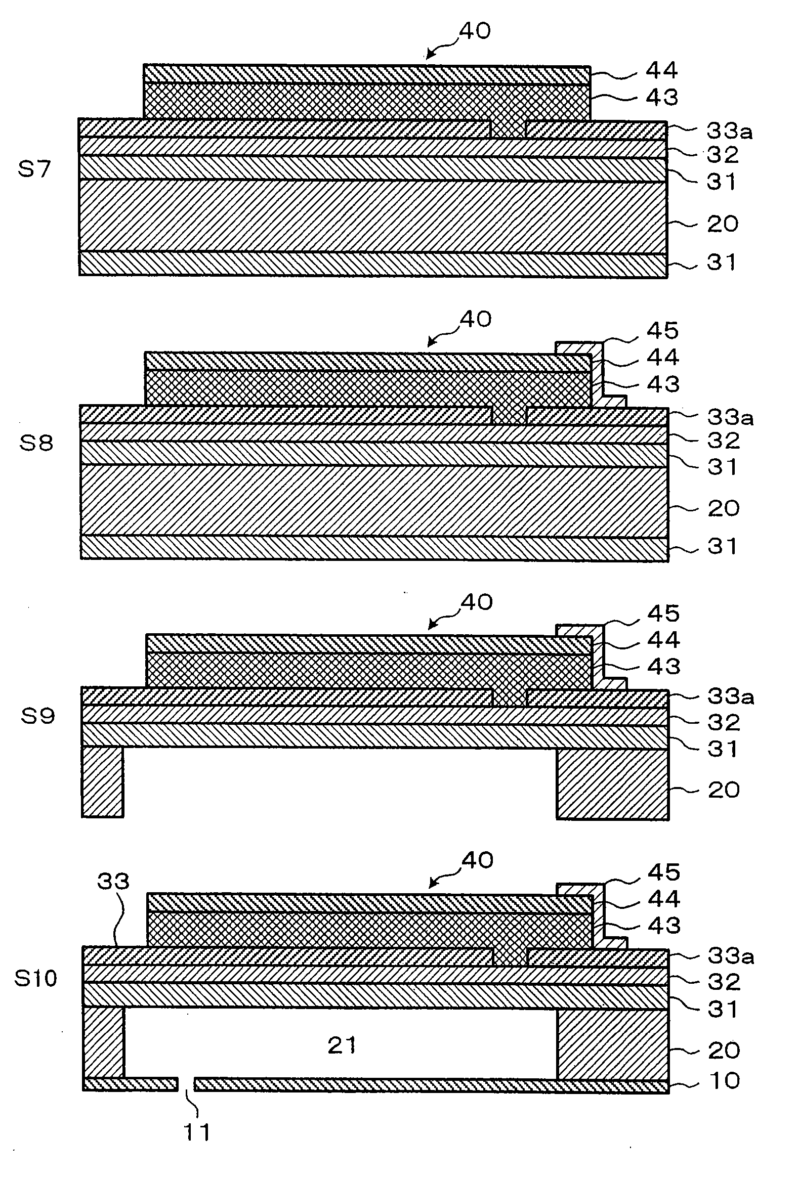
[0060] A method for the manufacture of the piezoelectric element in accordance with the present invention will be described below. FIGS. 5 and 6 are cross-sectional schematic views illustrating a method for the manufacture of the piezoelectric element and the ink-jet recording head of the first embodiment.

Step of Forming a Diaphragm (S1)

[0061] An insulating film 31 is formed on a silicon substrate 20. The thickness of the silicon substrate 20 is, for example, about 200 μm. In the manufacture of the insulating film, a high-temperature treatment is conducted in an oxidizing atmosphere composed of oxygen or steam and a film of silicon dioxide (SiO2) with a thickness of about 1 μm is formed. Besides the usually used thermal oxidation method, a CVD method can be used in this step.

[0062] Then, a ZrO2 film 32 with a thickness of about 400 nm is formed on the insulating film 31. The ZrO2 film 32 is obtained by growing a Zr layer by sputtering ...

second embodiment

Manufacturing Method of the Second Embodiment

[0084]FIG. 11 is a cross-sectional schematic view illustrating a method for the manufacture of the piezoelectric element and the ink-jet recording head of the second embodiment. This figure shows the part of the process corresponding to FIG. 5 of the first embodiment. In the process of the second embodiment, the steps other than the steps S3 through S5 of the first embodiment are the same as in the first embodiment and the explanation thereof is omitted.

Step of Forming a First Ti Layer (S3)

[0085] After the bottom electrode 33 of Ir and Pt is formed in the same manner as in S2 of the first embodiment, a step of forming a first Ti layer in which a Ti layer (nucleus) is formed on the bottom electrode 33 is immediately implemented. For example, a Ti layer is formed to a thickness of no less than 2 m and no more than 18 nm by a sputtering method or the like. The first Ti layer is formed uniformly on the bottom electrode 33, but it may also ...


PUM

PropertyMeasurementUnit
thicknessaaaaaaaaaa
thicknessaaaaaaaaaa
thicknessaaaaaaaaaa

Abstract

A piezoelectric element with stable and excellent piezoelectric properties is made by: a step of forming a diaphragm 30 (31, 32) on a substrate 20 (S1); a step of forming a bottom electrode 33 on the diaphragm 30 (S2); a step of forming a first piezoelectric layer 43a on the bottom electrode 33 (S3); a step of patterning both the piezoelectric layer 43a and the bottom electrode 33 (S4); a step of forming a second piezoelectric layer on the piezoelectric layer 43a and on the diaphragm 30 to mature a piezoelectric film 43 (S5); and a step of forming a top electrode 44 on the piezoelectric film 43 (S6).

Description

BACKGROUND OF THE INVENTION [0001] 1. Field of the Invention [0002] The present invention relates to a piezoelectric element having an electromechanical conversion function. In particular, the present invention relates to a piezoelectric element that makes it possible to obtain an excellent piezoelectric characteristic when used in an ink-jet recording head, a method for the manufacture thereof, and an ink-jet recording head and a printer using such piezoelectric elements. [0003] 2. Description of the Related Art [0004] Ink-jet recording heads use piezoelectric elements as driving mechanism for ink ejection in printers. The piezoelectric elements usually comprise a piezoelectric thin film and a top electrode and a bottom electrode disposed so as to sandwich the film. [0005] Piezoelectric elements with improved characteristics have been developed by regulating the crystal structure of a thin film composed of lead zirconium titanate (PZT) or forming Ti nuclei on the bottom electrode. ...

Claims


Application Information

Patent Timeline
Patent Type & Authority Applications(United States)
IPC IPC(8): H04R17/00H01G7/00B41J2/16H01L41/09H01L41/24
CPCB41J2/161Y10T29/49155B41J2/1628B41J2/1642B41J2/1645B41J2/1646B41J2002/14491H01L41/0973H01L41/318H01L41/319H01L41/332Y10T29/42Y10T29/49126Y10T29/49156Y10T29/49401Y10T29/435B41J2/1623H10N30/2047H10N30/078H10N30/079H10N30/082
Inventor MURAI, MASAMI
Owner SEIKO EPSON CORP
Why Eureka
Try Eureka