
Method of manufacturing a wiring board, a wiring board, a circuit element and a communications device

Active Publication Date: 2006-09-21
ORMON CORP
View PDF2 Cites 5 Cited by
  • Summary
  • Abstract
  • Description
  • Claims
  • Application Information

AI Technical Summary

Benefits of technology

[0020] Embodiments of the present invention provide a method of manufacturing a wiring board, a wiring board, a circuit element, and a communications device, which can reliably seal a space above a surface area containing at least a part of wiring.

Problems solved by technology

In particular, in the structure of coplanar type, as downsizing is easy to plan and electrical bonding strength between wires is weak, the coplanar type structure is often used in MEMS devices.
However, use of the above conventional manufacturing method leads to the problem that among MEMS switching elements 90 that have been simultaneously manufactured, a space containing a movable electrode 92 is not sealed completely in some MEMS switching elements 90.
In addition, a similar problem is generated in MEMS devices other than MEMS switching elements 90.

Method used


Image

  • Method of manufacturing a wiring board, a wiring board, a circuit element and a communications device
  • Method of manufacturing a wiring board, a wiring board, a circuit element and a communications device
  • Method of manufacturing a wiring board, a wiring board, a circuit element and a communications device

Examples


Embodiment Construction

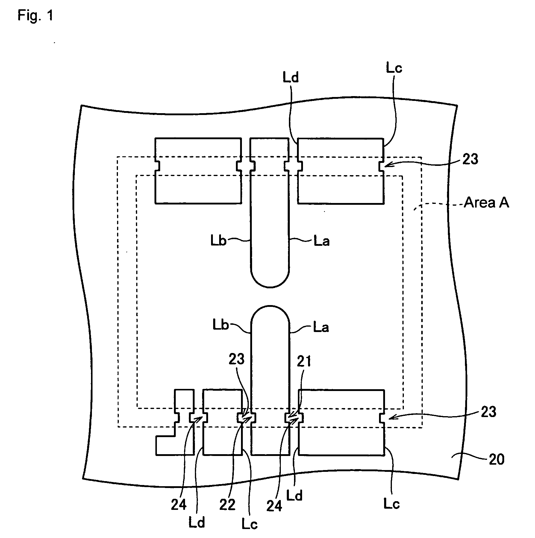
[0061] In the following, we describe one embodiment of the present invention with reference to either FIG. 1 or FIG. 21. First of all, we describe the schematic configuration of MEMS switching elements manufactured with a method of manufacturing according to the present embodiment. We will later describe details of the characteristic configuration of the MEMS switching element according to the present invention.

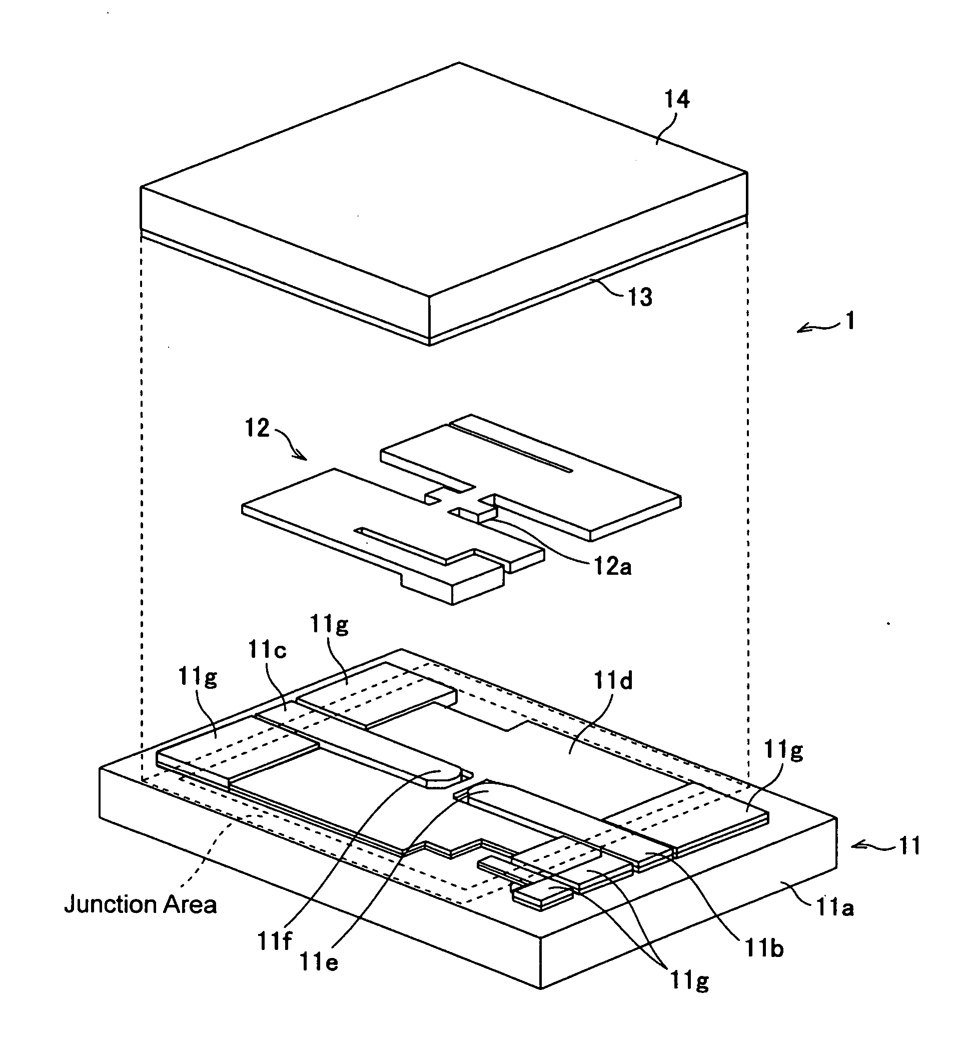
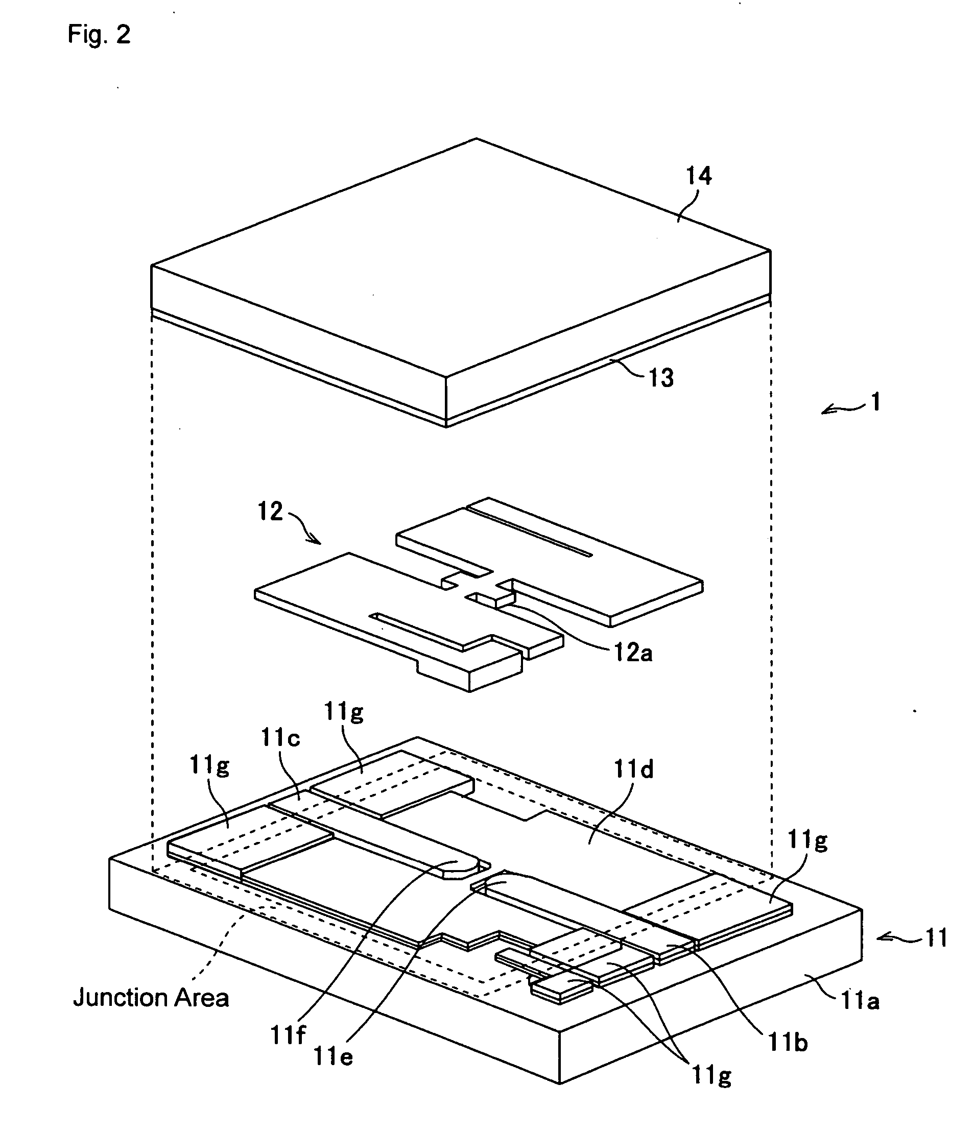
[0062] As shown in FIG. 2, a MEMS switching element (circuit element) 1 comprises a wiring board 11, a movable electrode (connection) 12, fritted glass (binder / sealed glass) 13, and a cap (lid) 14.

[0063] In addition, the wiring board 11 comprises a glass substrate 11a, signal lines (wires) 11b, 11c, a fixed electrode (GND) 11d, fixed contacts 11e, 11f, and bonding pads (wire / earthing conductor) 11g . . . The signal lines 11b, 11c, the fixed electrode 11d, the fixed contacts 11e, 11f, and the bonding pads 11g . . . are formed on the glass substrate 11a.

[0064] The movable el...


PUM

PropertyMeasurementUnit
Lengthaaaaaaaaaa
Electric potential / voltageaaaaaaaaaa
Widthaaaaaaaaaa

Abstract

A circuit element comprises a wiring board; the wiring board comprises a substrate and a wiring formed on the substrate, and a lid joined on the substrate containing a part of the wiring with a binder and making a sealed space above the substrate, wherein if a spot of the wiring joined with the lid by a binder is a spot of junction, a flank of both flanks of the wiring comprise bends in the spot of junction.

Description

BACKGROUND OF THE INVENTION [0001] 1. Field of the Invention [0002] The present invention relates to a method of manufacturing a wiring board, a photomask, a wiring board, a circuit element and a communications device. [0003] 2. Description of the Related Art [0004] A structure having the interior hermetically sealed by using sealed glass has been conventionally known. Among said structures, large ones include a cathode ray tube or a plasma display panel, for instance, and small ones include an SAW device or a crystal device. [0005] In addition, in recent years, high-frequency signals in GHz band for carrying out high-speed and large volume communications have come into use. For this reason, need for a high frequency device (hereinafter referred to as an MEMS device) by MEMS (Micro Electro Mechanical System) technique has increased. For instance, MEMS devices include such devices as a switch, a relay (switching element), a filter, a resonator, a phase shifter, etc. In such the MEMS ...

Claims


Application Information

Patent Timeline
IPC IPC(8): H05K7/06
CPCB81B2207/097B81C1/00301B81C1/00571B81C2201/0133B81C2201/0142Y10T29/49156B81C2203/036H05K7/06Y10T29/4913Y10T29/49126B81C2203/0109H01L2924/16235
Inventor MASAI, TAKUSANO, KOJI
Owner ORMON CORP
Learn More