Optical device

a technology of optical devices and optical light guides, applied in the field of optical devices, can solve the problems of limiting the number of wavelengths and imposing limits on the increase of interaction length, and achieve the effects of narrowing the pulse width, increasing the modulation index, and increasing the output wavelengths

Inactive Publication Date: 2006-09-21
FUJITSU LTD
View PDF3 Cites 25 Cited by
  • Summary
  • Abstract
  • Description
  • Claims
  • Application Information

AI Technical Summary

Benefits of technology

[0032] The above-described present invention primarily yields the following effects or advantages:
[0033] (1) The optical waveguide is formed in the substrate such that the light passing through the optical waveguide passes through, in a predetermined sequence, the position where the light passing through the optical waveguide is exposed to the electric field emitted from the signal electrode of the electrode section and the position where the light passing through the optical waveguide is exposed to the electric field converging at the ground electrode of the electrode section. Put another way, the optical waveguide is formed so as to pass through either an area under the electric field emission electrode or an area under the electric field convergence electrode, and then pass through the remaining electrode. Hence, the electric field emitted from the neighborhood of the signal electrode section and the electric field converging at the neighborhood of the ground electrode can be utilized for optical phase modulation. Even when the length of the waveguide (the length of interaction between light and electricity) is increased, the modulation index is increased by use of the electric field developing from the area under the ground electrode, thereby acquiring (increasing) a modulation index by the amount appropriate to the increase. Consequently, it becomes possible to increase the number of output wavelengths of the multiwavelength light source, to narrow the pulse width of the pulse light source, or to reduce the drive voltage (half wavelength voltage) for the multiwavelength light source and the pulse light source.
[0034] (2) When two ground electrodes are provided on respective sides of the signal electrode, the optical waveguide is formed so as to pass by the area under the signal electrode and the area under the respective ground electrodes, so that the modulation index can be increased while a longer interaction length is ensured.
[0035] (3) Further, the optical waveguide is formed on the substrate while being folded a plurality of times in the longitudinal direction of the substrate, so as to pass through an area under the ground electrode after having passed through the area under the signal electrode. As a result, even when a limitation is imposed on the size of the substrate, the modulation index can be increased while the longest-possible interaction length is ensured.

Problems solved by technology

However, since a ceiling is imposed on an output from the electrical amplifier, the number of wavelengths is limited.
However, a restriction is imposed on the size of the substrate, and hence a limit is imposed on an increase in interaction length.

Method used


Image

  • Optical device
  • Optical device
  • Optical device

Examples


first embodiment

[0048] [A] Description of First Embodiment

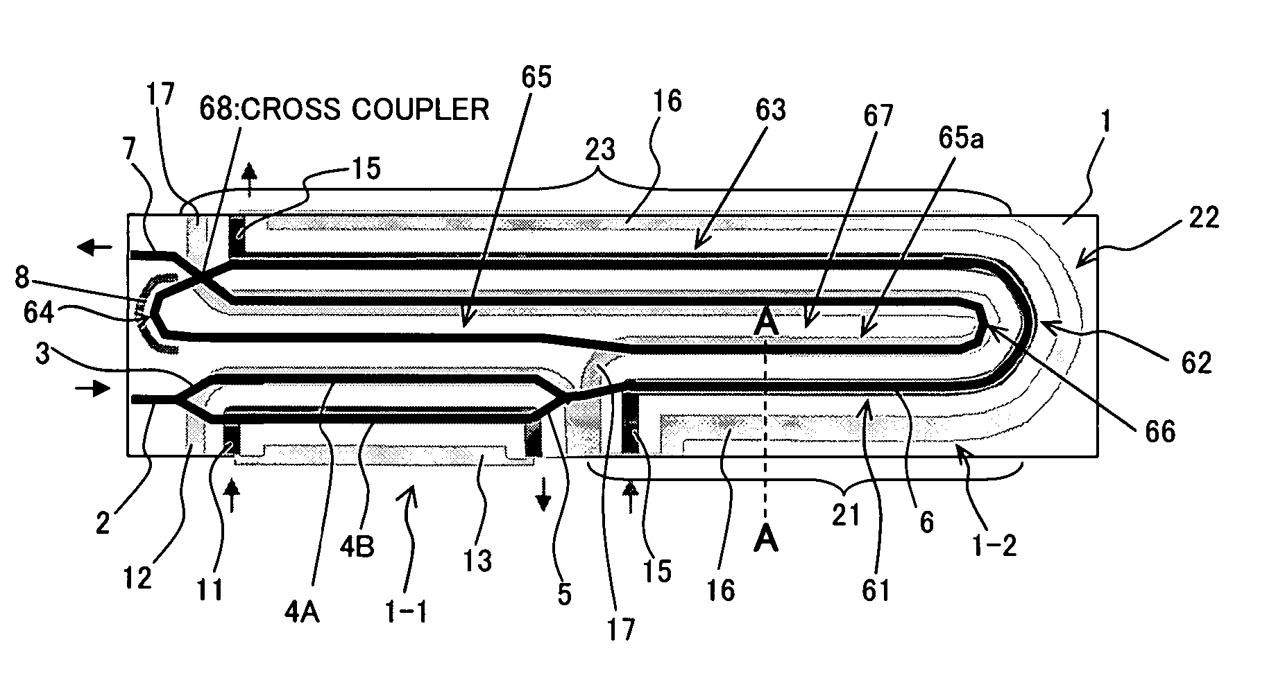
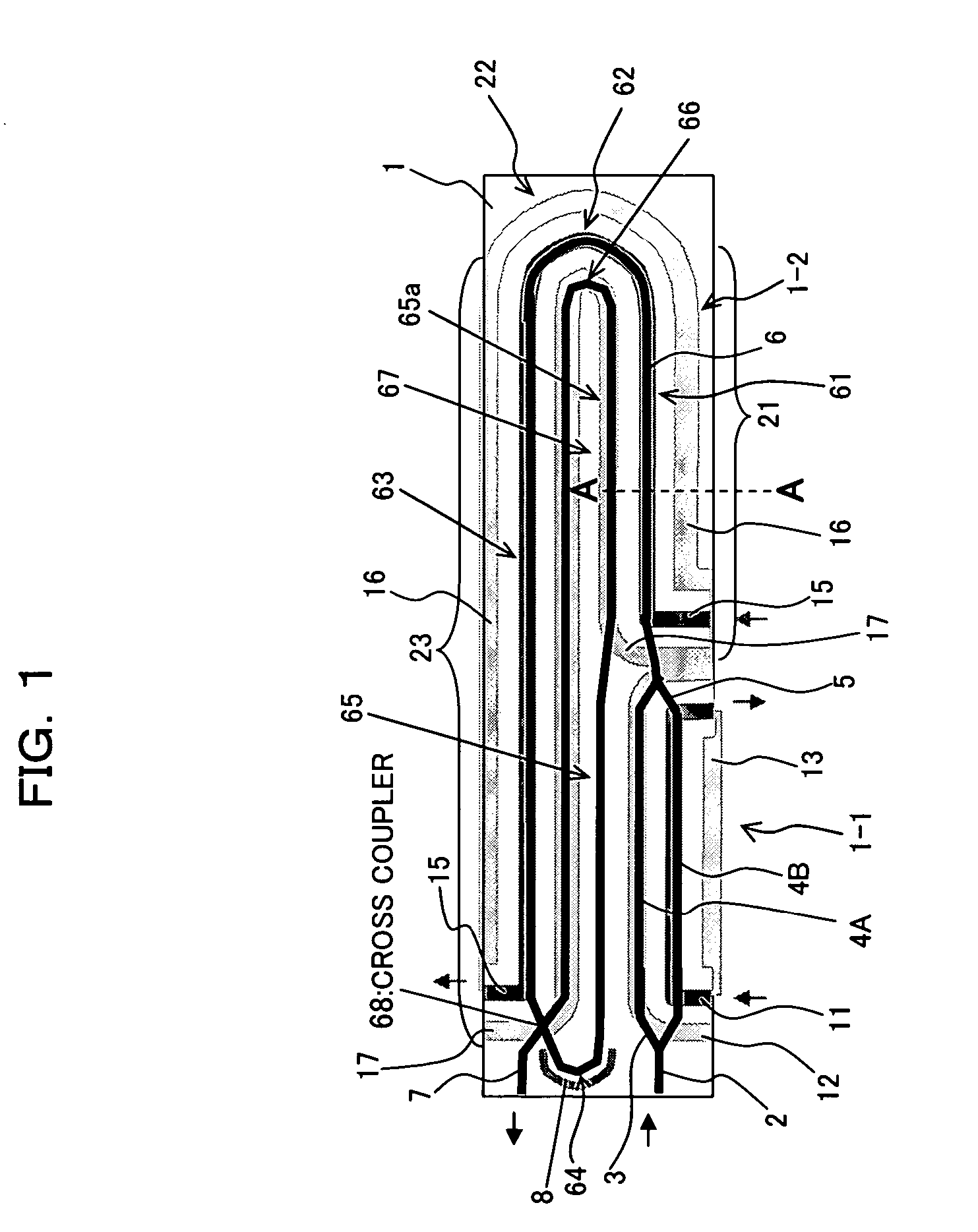
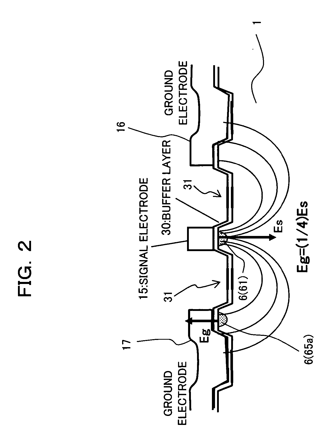
[0049]FIG. 1 is a schematic plan view showing the configuration of an optical modulator (an optical frequency comb generator) serving as an optical device according to a first embodiment of the present invention. FIG. 2 is a schematic cross-sectional view showing a cross sectional profile taken along A-A shown in FIG. 1 in conjunction with electric lines of force of an applied electric field. As shown in FIG. 1, the optical frequency comb generator of the present embodiment comprises a first optical modulator (an intensity modulator) 1-1 having a waveguide structure and a second optical modulator (a phase modulator) 1-2 connected in series with the intensity modulator 1-1, both of which are formed (integrated) on a substrate 1 exhibiting an electro-optical effect; e.g., an LN crystal or an LT crystal. The optical frequency comb generator can be applied as a multiwavelength light source (see FIG. 9), or as a pulse light source by addition of ...

second embodiment

[0107] [B] Description of a Second Embodiment

[0108]FIG. 6 is a schematic plan view showing the configuration of an optical modulator (a phase modulator) serving as an optical device according to a second embodiment of the present invention. In the phase modulator shown in FIG. 6, two parallel or essentially-parallel phase modulation waveguides (parallel waveguides) 6A, 6B are patterned on the substrate 1 having an electro-optical effect, such as an LN crystal or an LT crystal. The signal electrode (hot electrode) 15 is patterned on one (6B) of the parallel waveguides 6A, 6B. The earth electrodes (ground electrodes) 16, 17 parallel to the signal electrode 15 are patterned such that the signal electrode 15 is sandwiched therebetween. At this time, the earth electrode (ground electrode) 17 is patterned on the remaining one (6A) of the parallel waveguides 6A, 6B.

[0109] As a result, the signal electrode 15 which is arranged to partially overlap one (6B) of the parallel waveguides 6A, 6B...


PUM

PropertyMeasurementUnit
frequencyaaaaaaaaaa
widthaaaaaaaaaa
thicknessaaaaaaaaaa

Abstract

An optical device having a substrate having an electro-optical effect, an optical waveguide formed in the substrate, and an electric field emission electrode, and an electric field convergence electrode to which an electric field emitted from the electric field emission electrode converges. The optical waveguide is formed such that light propagating through the optical waveguide passes through an area under the electric field emission electrode or an area under the electric field convergence electrode and then passes through a remaining electrode. As a result, even when an interaction length is increased, the optical device acquires (increases) a modulation index appropriate to the increase in interaction length, thereby diminishing a drive voltage.

Description

CROSS REFERENCE TO RELATED APPLICATIONS [0001] This application is based on and hereby claims priority to Japanese Application No. 2005-79699 filed on Mar. 18, 2005 in Japan, the contents of which are hereby incorporated by reference. BACKGROUND OF THE INVENTION [0002] (1) Field of the Invention [0003] The present invention relates to an optical device used for optical communication, and more particularly, to a technique suitable for use in an optical device, such as an optical modulator having an optical waveguide structure. [0004] (2) Description of Related Art [0005] An optical communications device typified by an optical modulator using an electro-optical crystal, such as an LiNbO3 [lithium niobate (LN)] crystal substrate or an LiTaO2 [lithium tantalate (LT)] crystal substrate, is formed by placing electrodes in the vicinity of an optical waveguide after a metal film has been formed over a portion of the crystal substrate and then the film has been thermally diffused, or after a...

Claims


Application Information

Patent Timeline
Patent Type & Authority Applications(United States)
IPC IPC(8): G02F1/035
CPCG02F1/035G02F1/2255G02F2203/54
Inventor SUGIYAMA, MASAKI
Owner FUJITSU LTD
Why Eureka
Try Eureka