Non-volatile memory structure and method of fabrication

a memory structure and non-volatile technology, applied in the direction of basic electric elements, semiconductor devices, electrical equipment, etc., can solve the problems of poor quality, easy breakdown, and inability to integrate bit line oxides b>, and achieve the effect of increasing the effective width leff of the channel without increasing the feature siz

Active Publication Date: 2006-09-21
SAIFUN SEMICON
View PDF99 Cites 27 Cited by
  • Summary
  • Abstract
  • Description
  • Claims
  • Application Information

AI Technical Summary

Benefits of technology

[0010] An object of the present invention is, at least, to increase the effective width Leff of the channel without increasing the feature size.
[0014] Still further, in accordance with a preferred embodiment of the present invention, generating bit lines includes implanting the bit lines and performing a rapid thermal anneal.

Problems solved by technology

A common problem is the integrity of bit line oxides 26.
In general, middles 25 are of good quality but beaks 27 are of poor quality, and thus are susceptible to breakdown.
Moreover, the thickness of middles 25 is sensitive to the concentration of n+ doping at the surface of bit line 22 and is thus, difficult to control.
However, this causes substantial thermal drive, which increases the side diffusion of bit lines 22.
Another common problem is that the NROM manufacturing process is significantly different than the periphery CMOS manufacturing process but, to create a wafer with both CMOS and NROM elements, both processes are integrated together.
Unfortunately, some of the bit lines occasionally do not reach the first polysilicon layer.

Method used


Image

  • Non-volatile memory structure and method of fabrication
  • Non-volatile memory structure and method of fabrication
  • Non-volatile memory structure and method of fabrication

Examples


Embodiment Construction

[0047] In the following detailed description, numerous specific details are set forth in order to provide a thorough understanding of the invention. However, it will be understood by those skilled in the art that the present invention may be practiced without these specific details. In other instances, well-known methods, procedures, and components have not been described in detail so as not to obscure the present invention.

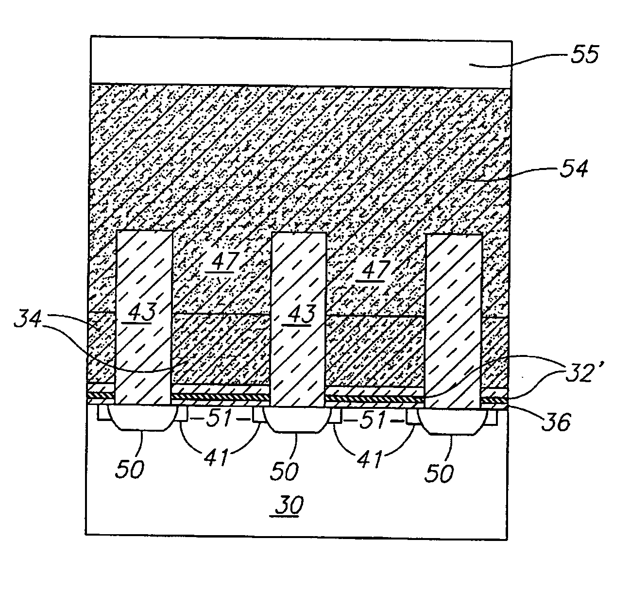
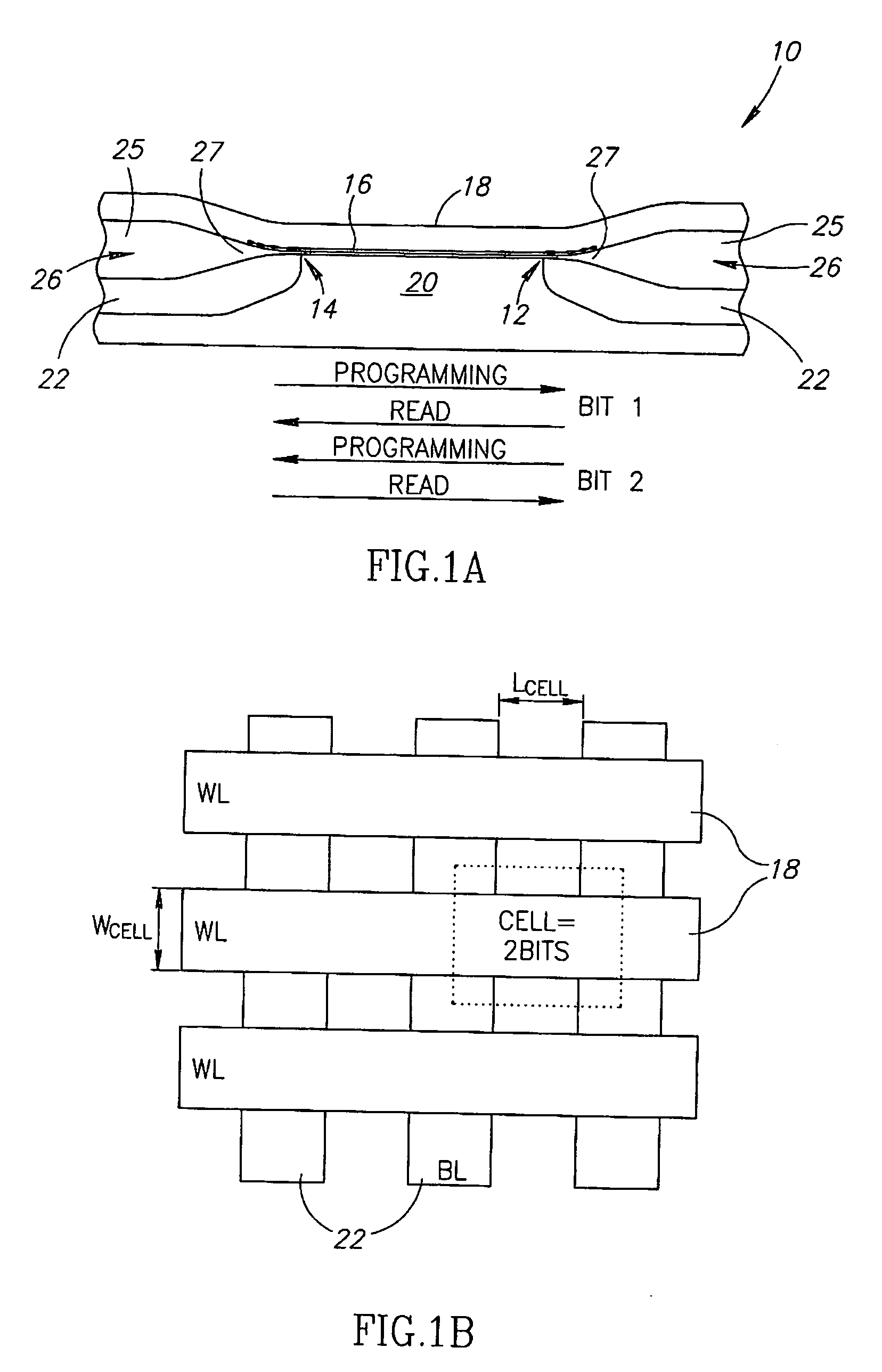
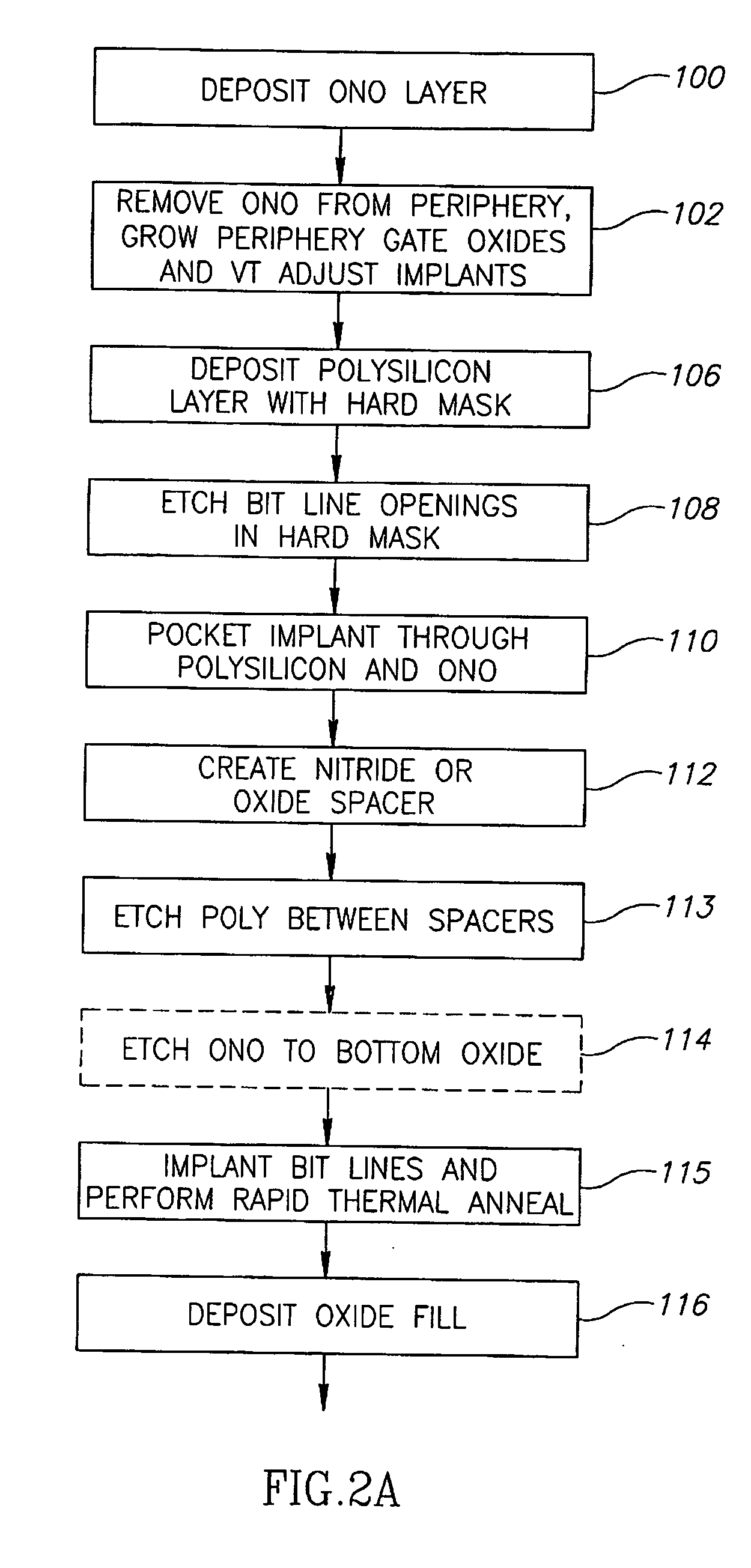
[0048] Reference is now made to FIGS. 2A and 2B, which, together, illustrate a novel process for manufacturing nitride read only memory (NROM) arrays which may attempt to ensure the presence of an overlap at the junction of the bit lines with the polysilicon gates. Reference is also made to FIGS. 3A-3I which show the results of various steps of FIG. 2 and to FIGS. 4A and 4B which show the layout of various steps of FIG. 2. As is discussed in more detail hereinbelow, the present invention may provide a smaller cell size and, with the more reliable overlap, the pr...


PUM


Abstract

A method for creating a non-volatile memory array includes implanting pocket implants in a substrate at least between mask columns of a given width and at least through an ONO layer covering the substrate, generating increased-width polysilicon columns from the mask columns, generating bit lines in the substrate at least between the increased-width polysilicon columns and depositing oxide at least between the polysilicon columns.

Description

CROSS-REFERENCE TO RELATED APPLICATIONS [0001] The present application is a continuation-in-part application claiming benefit from U.S. patent application Ser. No. 11 / 247,733, filed Oct. 11, 2005, which application claims benefit from U.S. Provisional Patent Application 60 / 618,165, filed Oct. 14, 2004, which applications are hereby incorporated in their entirety by reference.FIELD OF THE INVENTION [0002] The present invention relates to volatile memory devices, such as nitride read only memory (NROM) cells generally and to their structure and methods of fabrication in particular. BACKGROUND OF THE INVENTION [0003] Dual bit memory cells are known in the art. One such memory cell is the NROM (nitride read only memory) cell 10, shown in FIG. 1A to which reference is now made, which stores two bits 12 and 14 in a nitride based layer 16, such as an oxide-nitride-oxide (ONO) stack, sandwiched between a polysilicon word line 18 and a channel 20. Channel 20 is defined by buried bit line dif...

Claims


Application Information

Patent Timeline
Patent Type & Authority Applications(United States)
IPC IPC(8): H01L21/8238H01L21/3205H01L21/31
CPCH01L21/28282H01L27/115H01L27/11568H01L29/66833H01L21/32139H01L29/40117H10B43/30H10B69/00
Inventor LUSKY, ELISHAPPIR, ASSAFIRANI, RUSTOMEITAN, BOAZ
Owner SAIFUN SEMICON
Why Eureka
Try Eureka