Substrate stiffness method and resulting devices for layer transfer process

a technology of layer transfer and substrate, which is applied in the manufacture of microstructured devices, semiconductor devices, electrical equipment, etc., can solve the problems of difficult to achieve the effect of separating or cutting extremely hard and/or brittle materials, and achieving the effect of maintaining the effective deflection characteristic, suitable deflection characteristic, and effective deflection

a technology of layer transfer and substrate, which is applied in the manufacture of microstructured devices, semiconductor devices, electrical equipment, etc., can solve the problems of difficult to achieve the effect of separating or cutting extremely hard and/or brittle materials, and achieving the effect of maintaining the effective deflection characteristic, suitable deflection characteristic, and effective deflection

US20060211219A1Active Publication Date: 2006-09-21SILICON GENERAL CORPORATION

Image

  • Substrate stiffness method and resulting devices for layer transfer process
  • Substrate stiffness method and resulting devices for layer transfer process
  • Substrate stiffness method and resulting devices for layer transfer process

Examples


examples

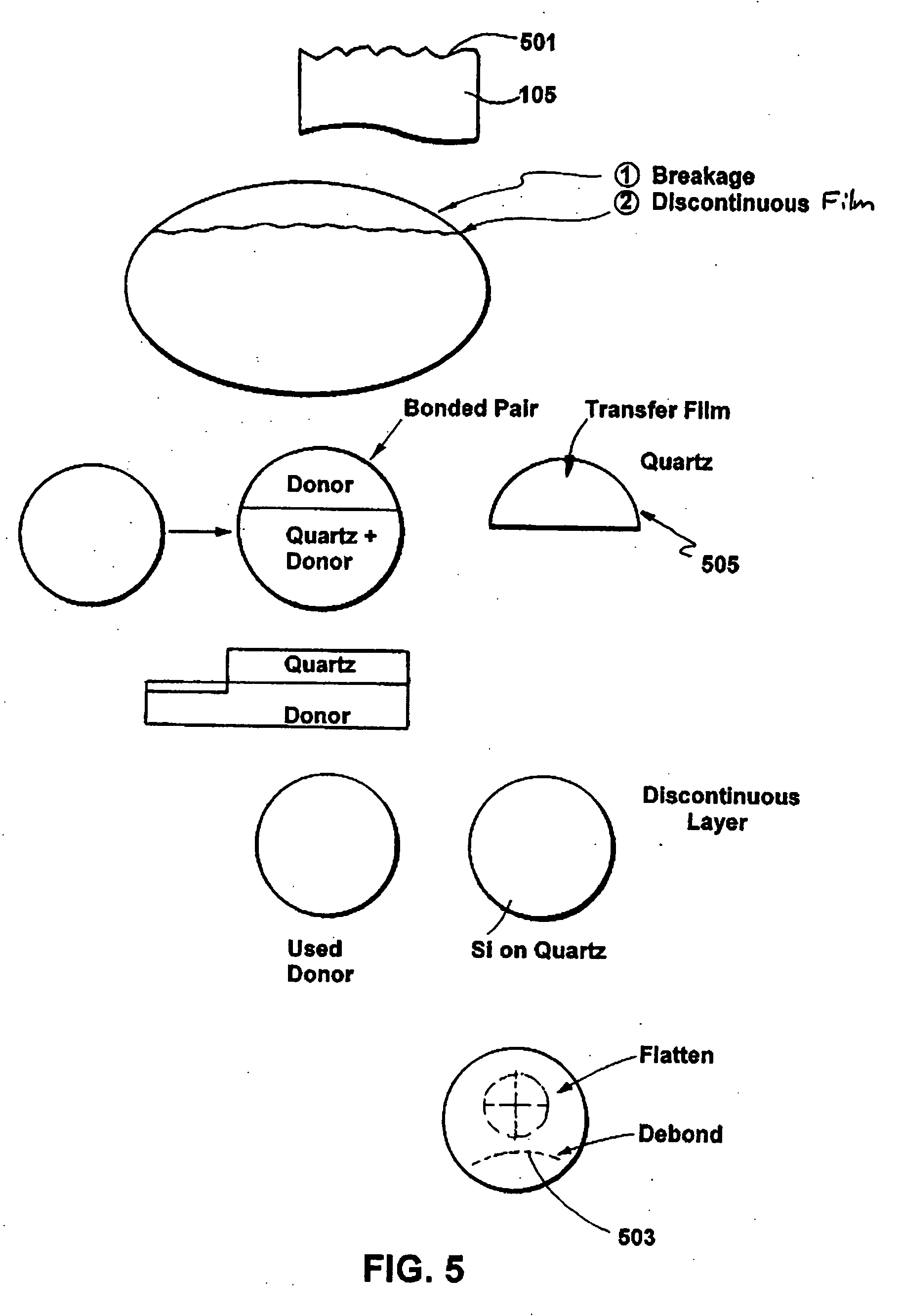
[0235] To prove the principle and operation of the present invention, we performed various experiments using certain calculations. These experiments are merely examples, which should not unduly limit the scope of the claims herein. One of ordinary skill in the art would recognize many variations, modifications, and alternatives. Referring to FIG. 48 through 50, we have provided an example using a silicon substrate 4801, a quartz substrate 4803, and a backing layer 4905, which is called the “added layer.” As also shown, a cantilever of length, L 4807, operated upon by an end force, F, should have a deflection given by:

Deflection=F*Lˆ3 / (3*E*I)   Equation 1

[0236] where F is the force operating at the cantilever end;

[0237] where I is the AREA moment of inertia of the beam; and

[0238] E is the Young's modulus.

[0239] In the present example, quartz and silicon have different E values. Quartz and silicon also have slightly different thicknesses. Accordingly, we expect a bending characte...


PUM


Abstract

A method and structures for manufacturing multi-layered substrates. The method includes providing a donor substrate, which has a first deflection characteristic. The donor substrate has a backside, a face, a cleave region, and a thickness of material defined between the cleave region and the face. The method includes bonding the face of the donor substrate to a face of the handle substrate. The method includes coupling a backing substrate to the backside of the donor substrate to form a multilayered structure. The backing substrate is adequate to cause the first deflection characteristic of the donor substrate to be reduced to a predetermined level. The predetermined level is a suitable deflection characteristic for the thickness of material to be transferred onto the face of a handle substrate. The method includes initiating a controlled cleaving process within a portion of the cleave region of the donor substrate to begin removal of the thickness of material from the donor substrate at a portion of the cleave region, while the backing substrate remains attached to the donor substrate to maintain at least the suitable deflection characteristic.

Description

CROSS-REFERENCES TO RELATED APPLICATIONS [0001] The instant nonprovisional patent application claims priority to U.S. provisional patent application No. 60 / 657,558 filed Feb. 28, 2005, and U.S. provisional patent application No. 60 / 657,262 filed Feb. 28, 2005, both of which are incorporated by reference herein for all purposes.BACKGROUND OF THE INVENTION [0002] The present invention relates to the manufacture of substrates. More particularly, the invention provides a technique including a method and a structure for forming multi-layered substrate structures for the fabrication semiconductor integrated circuits, for example. But it will be recognized that the invention has a wider range of applicability; it can also be applied to other substrates for multi-layered integrated circuit devices, three-dimensional packaging of integrated semiconductor devices, photonic and / or optoelectronic devices, piezoelectronic devices, microelectromechanical systems (“MEMS”), nano-technology structur...

Claims


Application Information

Patent Timeline
21 Sep 2006
Publication
US20060211219A1
IPC
H01L21/30; H01L21/46
CPC
B81C1/00357; B81C2201/019; H01L2221/68359; H01L21/6835; H01L21/76254; H01L21/2007; H01L21/20
Inventors
HENLEY, FRANCOIS J.; KIRK, HARRY ROBERT