

Package, and fabrication method for the package
a technology of packaging and fabrication method, applied in the direction of electrical equipment, semiconductor devices, semiconductor/solid-state device details, etc., can solve the problems of reduced electrical performance, insufficient heat radiation, electric conduction, etc., and achieve the effect of improving reliability, simple configuration, and easy processing fabrication
- Summary
- Abstract
- Description
- Claims
- Application Information
AI Technical Summary
Benefits of technology
Problems solved by technology
Method used
Image

Examples
first embodiment
Package Structure
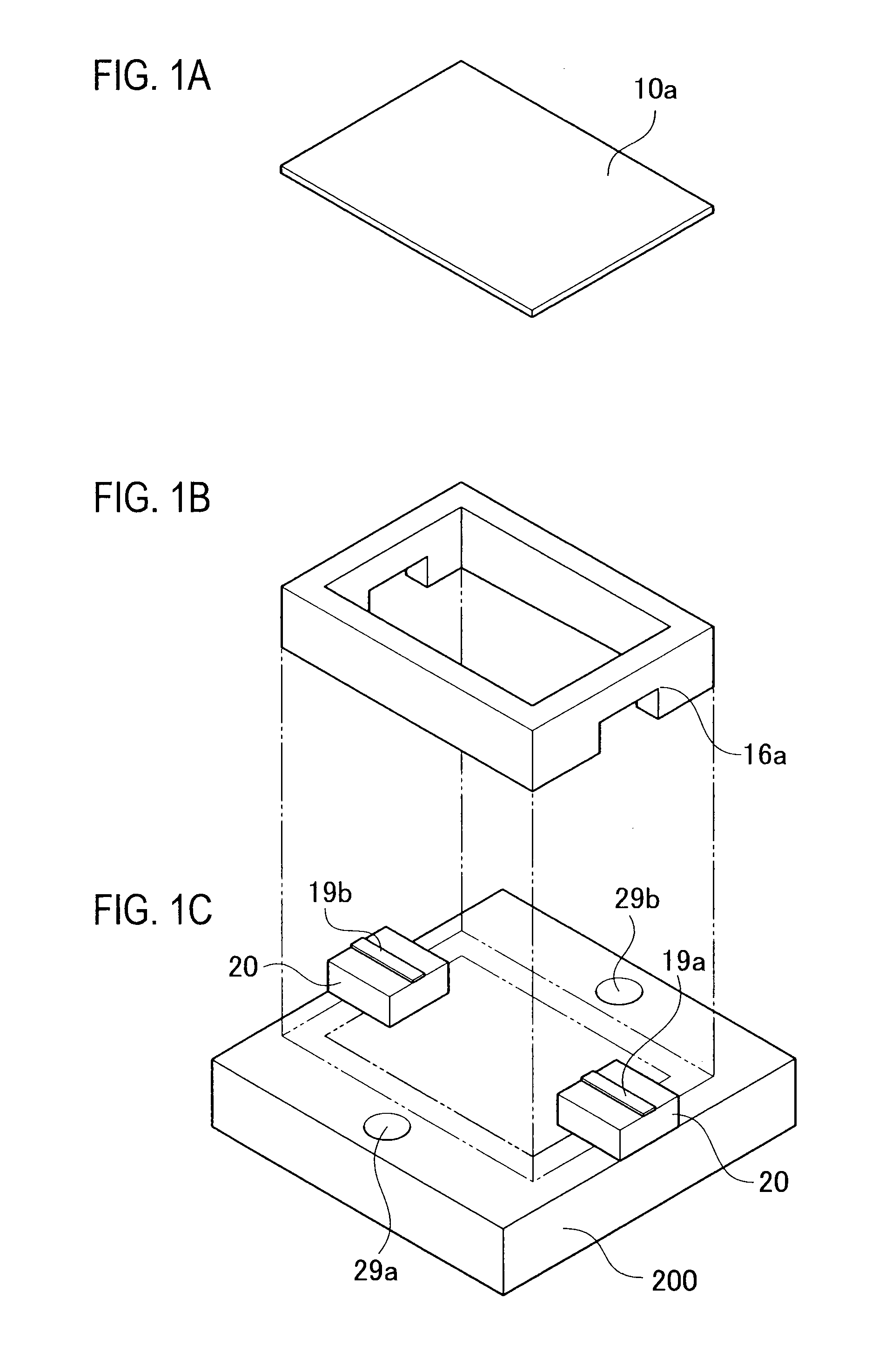
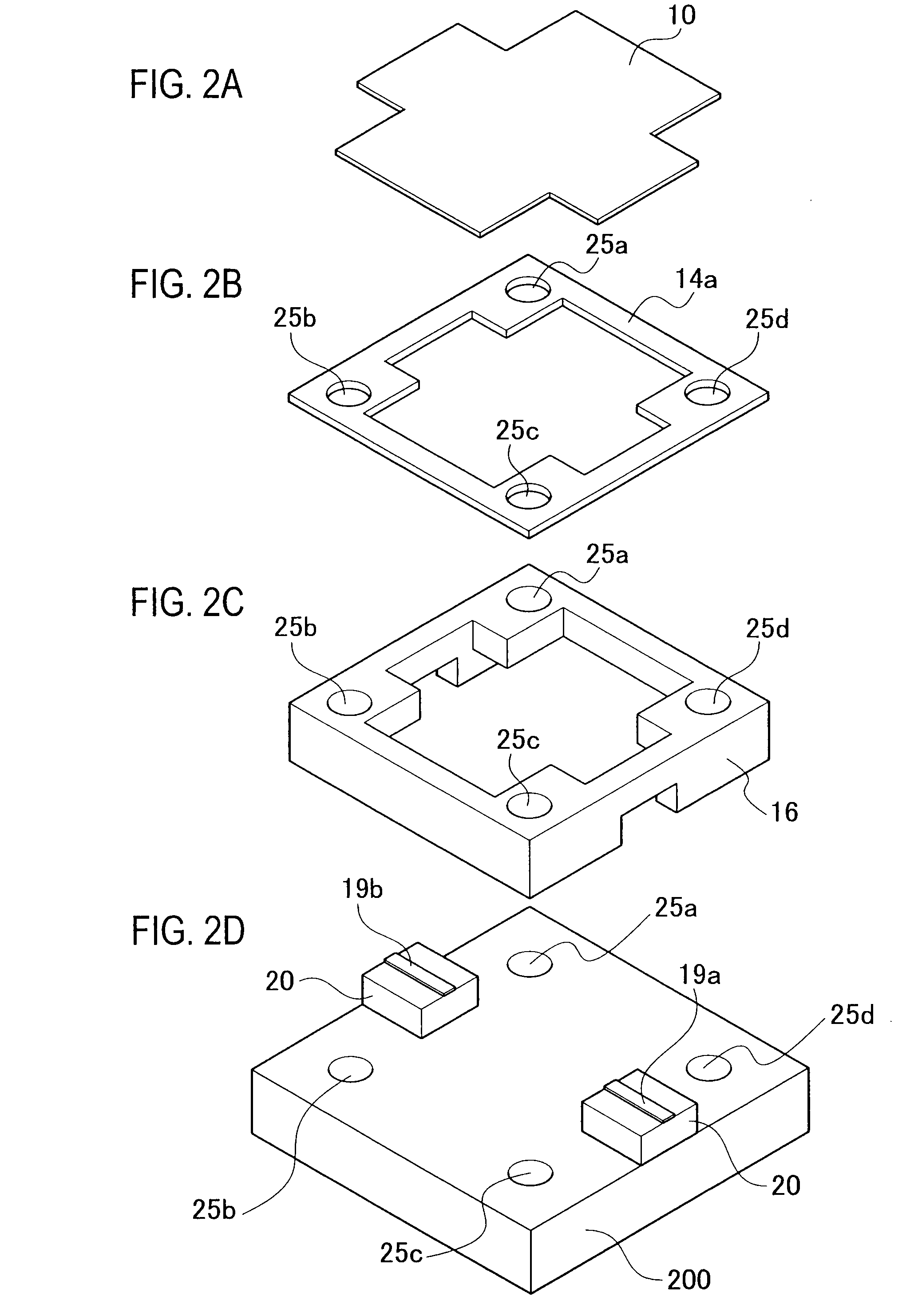
[0055]A schematic bird' s-eye view for explaining a fabrication method of a package according to a first embodiment of the present invention is expressed as shown in FIG. 2. FIG. 2A shows a schematic configuration of a ceramic cap 10. FIG. 2B shows a schematic configuration of a metal seal ring 14a having screw holes 25a to 25d in a corner part. FIG. 2C shows a schematic configuration of a ceramic wall 16 having the screw holes 25a to 25d to a corner part. FIG. 2D shows a schematic configuration of an input stripline 19a and an output stripline 19b disposed on a conductive base plate 200 and an insulating layer 20.
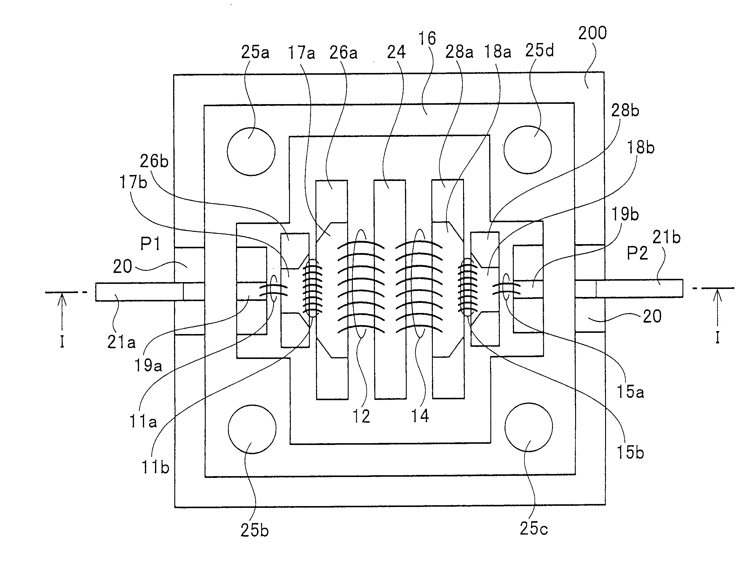
[0056]As shown in FIG. 2, the package according to the first embodiment includes: a ceramic cap 10 having a cross form shaped plate; a metal seal ring 14a of the framed shape having a cross type apertural area; a ceramic wall 16 of the frame shape having a cross type apertural area; and an input stripline 19a and an output stripline 19b disposed on a condu...
modified example 1 of first embodiment
[0079]As shown in FIG. 5, a schematic plane pattern configuration of a package according to the modified example 1 of the first embodiment is composed of two stage constitution of amplifiers. A first stage amplifier includes: a conductive base plate 200; a semiconductor device 24 disposed on the conductive base plate 200; and an input circuit substrates 26a and 26b and the output circuit substrates 28a and 28b disposed on the conductive base plate 200, adjoining of the semiconductor device 24. A second stage amplifier is also provided with the same configuration. As shown in FIG. 5, a stripline 19c is disposed at the connected portion between the first stage amplifier and the second stage amplifier, and the stripline 19c connects an output matching circuit 18b of the first stage amplifier and an input matching circuit 17b of the second stage amplifier.
[0080]As shown in FIG. 5, a package according to the modified example 1 of the first embodiment includes: the conductive base plate 2...
modified example 2 of first embodiment
[0088]A schematic plane pattern configuration of a package according to a modified example 2 of the first embodiment is expressed as shown in FIG. 6.
[0089]In the package according to the modified example 2 of the first embodiment, the ceramic wall 16 has a polygonal shape hollow area by forming the corner part of frame shape thickly, and forming the side part of frame shape in linear shape.
[0090]Since it is only that the configuration of the package according to the modified example 2 of the first embodiment differs in the shape of the ceramic wall 16, and other configurations are the same as that of the first embodiment, the duplicate explanation is omitted.
[0091]The polygon may be any one of a hexagon or an octagon.
[0092]According to the package according to the modified example 2 of the first embodiment, as for the shape of the hollow area of the ceramic wall 16, the frame shape of the ceramic wall 16 can be directly screw fastened to the conductive base plate 200 in the corner p...
PUM
| Property | Measurement | Unit |
|---|---|---|
| frequency | aaaaa | aaaaa |
| length W3 | aaaaa | aaaaa |
| length W3 | aaaaa | aaaaa |
Abstract
Description
Claims
Application Information