Deposition system and method

a technology of deposition system and deposited film, which is applied in the direction of chemical vapor deposition coating, coating, electric discharge tube, etc., can solve the problems of affecting the quality of deposited films, current ald processes, and generally slow deposition rate that is not feasible for production requirements, so as to reduce contamination problems

Active Publication Date: 2006-09-21
TOKYO ELECTRON LTD
View PDF13 Cites 361 Cited by
  • Summary
  • Abstract
  • Description
  • Claims
  • Application Information

AI Technical Summary

Benefits of technology

[0008] Another object of the present invention is to red...

Problems solved by technology

In addition, plasma excitation may activate film-forming chemical reactions that are not energetically or kinetically favored in thermal CVD.
However, current ALD processes generally have a slow deposition rate that is not feasible for production requirements.
Mor...

Method used


Image

  • Deposition system and method
  • Deposition system and method
  • Deposition system and method

Examples


Embodiment Construction

[0031] In the following description, in order to facilitate a thorough understanding of the invention and for purposes of explanation and not limitation, specific details are set forth, such as a particular geometry of the deposition system and descriptions of various components. However, it should be understood that the invention may be practiced in other embodiments that depart from these specific details.

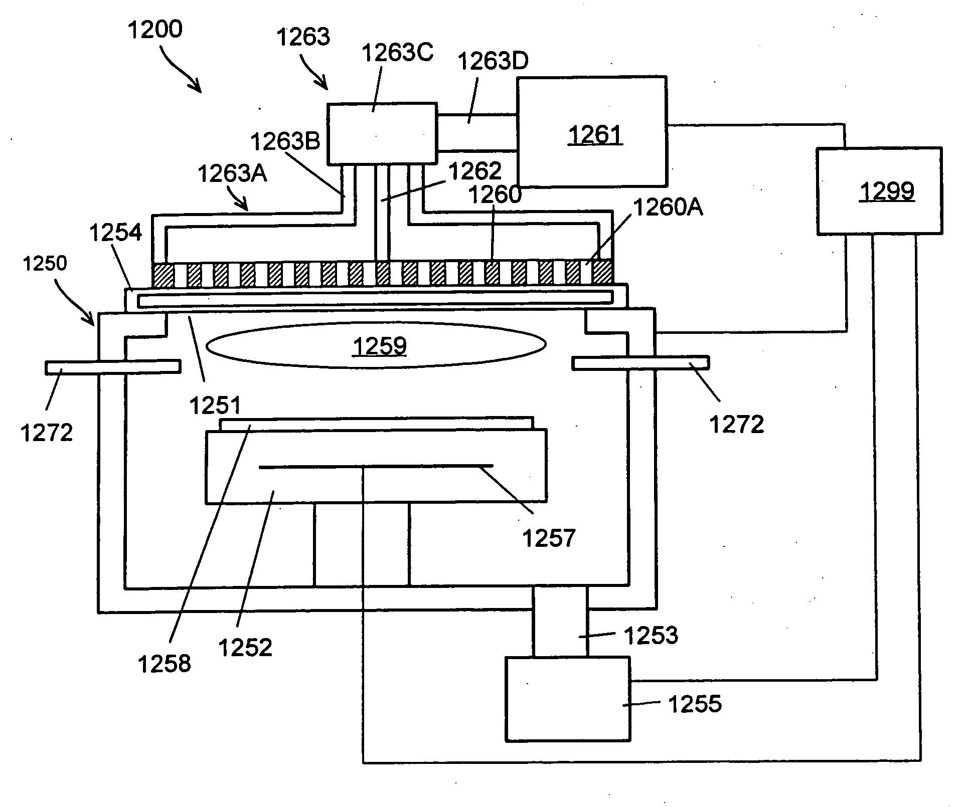
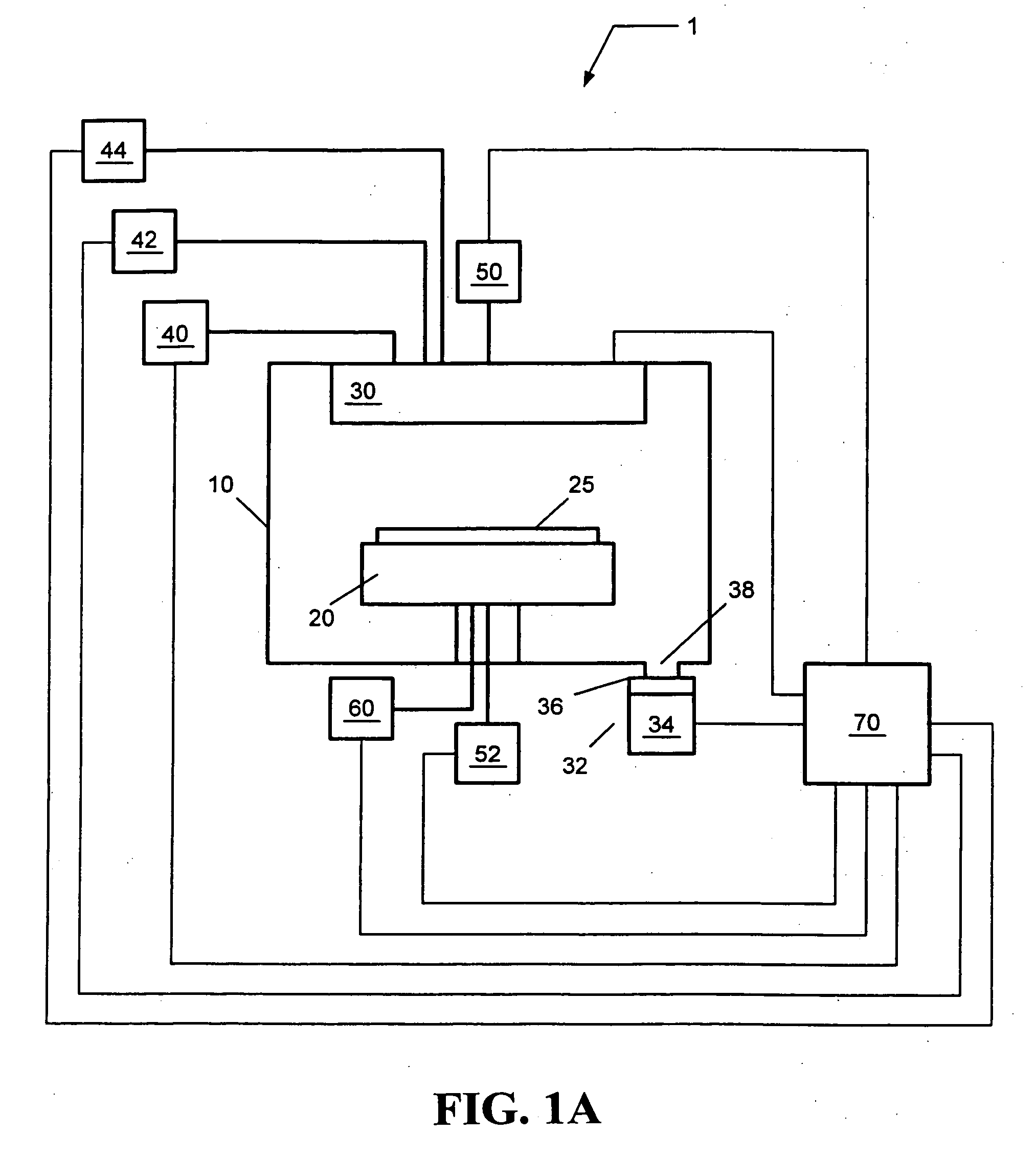
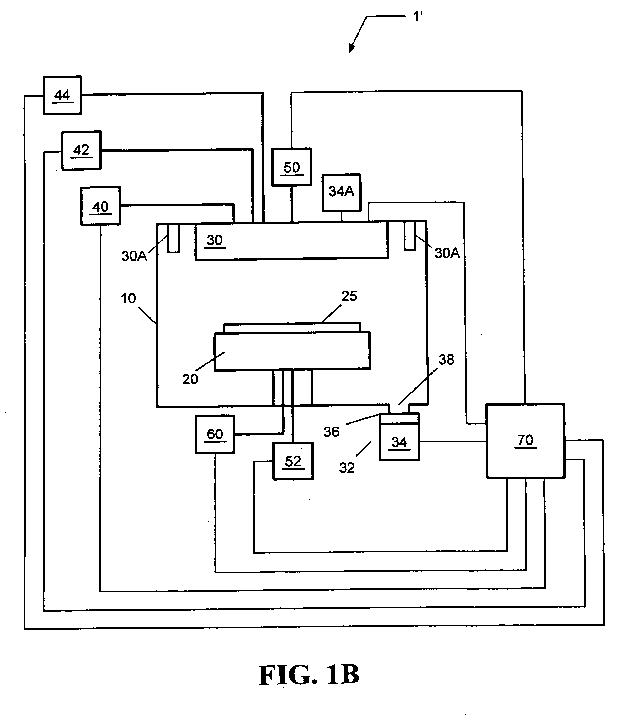
[0032] Referring now to the drawings, wherein like reference numerals designate identical or corresponding parts throughout the several views, FIG. 1A illustrates a deposition system 1 for depositing a thin film on a substrate according to one embodiment. For example, during the metallization of inter-connect and intra-connect structures for semiconductor devices in back-end-of-line (BEOL) operations, a thin conformal barrier layer may be deposited on wiring trenches or vias to minimize the migration of metal into the inter-level or intra-level dielectric. Further, a thin confor...


PUM

PropertyMeasurementUnit
Poweraaaaaaaaaa
Energyaaaaaaaaaa
Timeaaaaaaaaaa

Abstract

A method for processing a substrate includes disposing the substrate in a deposition chamber configured to perform a deposition process and depositing a film on the substrate using the deposition process. The substrate having the film thereon is then transferred from the deposition chamber into a treatment chamber and a plasma cleaning process is performed on the substrate in the treatment chamber. Further processing of the substrate is performed after the plasma cleaning process.

Description

BACKGROUND OF THE INVENTION [0001] 1. Field of the Invention [0002] The present invention relates to a deposition system and a method of operating thereof, and more particularly to a deposition system having reduced contamination. [0003] 2. Description of Related Art [0004] Typically, during materials processing, plasma is employed to facilitate the addition and removal of material films when fabricating composite material structures. For example, in semiconductor processing, a (dry) plasma etch process is utilized to remove or etch material along fine trenches or within vias or contacts patterned on a silicon substrate. Alternatively, for example, a vapor deposition process is utilized to deposit material along fine lines or within vias or contacts on a silicon substrate. In the latter, vapor deposition processes include chemical vapor deposition (CVD), and plasma enhanced chemical vapor deposition (PECVD). [0005] In PECVD, plasma is utilized to alter or enhance the film deposition...

Claims


Application Information

Patent Timeline
IPC IPC(8): H01L21/44
CPCC23C16/14H01L21/76843C23C16/34C23C16/45538C23C16/45544C23C16/5096H01J37/32082H01J37/32192H01J2237/335H01L21/28562H01L21/3141H01L21/31608H01L21/31616H01L21/31637H01L21/31641H01L21/31645H01L21/318H01L21/32051C23C16/303H01L21/02271H01L21/0228H01L21/02274
Inventor ISHIZAKA, TADAHIROLUDVIKSSON, AUDUNN
Owner TOKYO ELECTRON LTD
Why Eureka
Try Eureka