Semiconductor device and manufacturing method thereof

Inactive Publication Date: 2006-09-28
RENESAS TECH CORP
View PDF5 Cites 3 Cited by
  • Summary
  • Abstract
  • Description
  • Claims
  • Application Information

AI Technical Summary

Benefits of technology

[0021] It is possible to optimize the threshold voltages of a nMOS transistor and a pMOS transistor using a gate insulator made of a hafnium-based high-k material.

Problems solved by technology

As described in the patent document 1, the MOS transistor in which a gate insulator is formed of hafnium oxide has a problem that the low-voltage operation thereof is difficult due to the Fermi-level pinning, in which silicon atoms and hafnium atoms are bonded at the interface with the polycrystalline silicon gate electrode to form a level and thus the threshold voltage is increased.
However, since the thickness of at least 1 to 2 nm or more is required in order to produce the sufficient effect of the barrier layer, another problem that the effective dielectric constant of a gate insulator is reduced occurs.
Also, since a silicon nitride film has positive fixed potential and an alumina film has negative fixed potential, a steep interface is formed between the barrier layer and the gate insulator to develop a defect, and the problem of the degradation of electrical properties of the MOS transistor occurs.
Furthermore, there is also a problem that the hysteresis of the capacitance-voltage (C-V) properties is increased in proportion to the thickness of the barrier layer.

Method used


Image

  • Semiconductor device and manufacturing method thereof
  • Semiconductor device and manufacturing method thereof
  • Semiconductor device and manufacturing method thereof

Examples


first embodiment

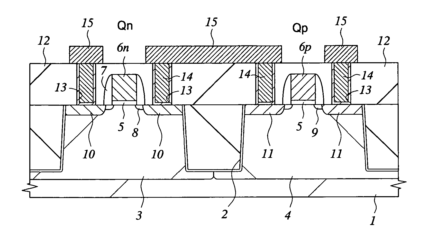
[0034]FIG. 1 is a cross-sectional view of the principal part of a semiconductor substrate showing a CMOS circuit (circuit composed of a nMOS transistor Qn and a pMOS transistor Qp) according to the first embodiment.

[0035] For example, the nMOS transistor Qn is formed on a p type well 3 in a semiconductor substrate (hereinafter, referred to as a substrate) 1 made of p type single crystal silicon, and the pMOS transistor Qp is formed on a n type well 4 in the substrate 1. The p type well 3 and the n type well 4 are isolated from each other by a device isolation trench 2 formed in the substrate 1.

[0036] The nMOS transistor Qn is provided with a gate insulator 5 formed on the p type well 3, a gate electrode 6n made of a n type polycrystalline silicon film formed on the gate insulator 5, and a source and a drain formed near the surface of the p type well 3. The source and drain are formed to have a LDD (Lightly Doped Drain) structure composed of a pair of n+ semiconductor regions 10 an...

second embodiment

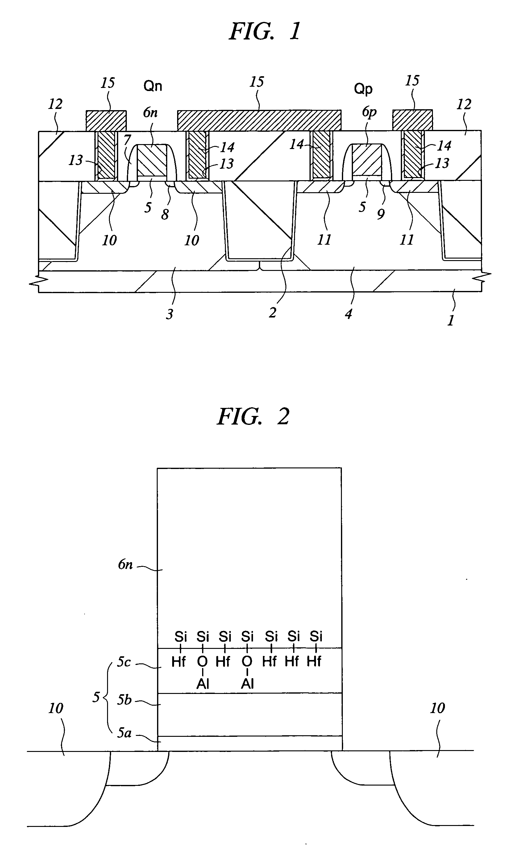
[0055]FIG. 11 is an enlarged cross-sectional view of the principal part showing a gate insulator 5 and a gate electrode 6n of a nMOS transistor Qn according to the second embodiment.

[0056] The gate insulator 5 of the nMOS transistor Qn according to this embodiment is composed of a thin silicon oxide film 5a with a thickness of about 0.4 to 1.5 nm and a HfAlOx film 5d with a thickness of about 2.5 to 5.0 nm formed on the silicon oxide film 5a. Similar to the first embodiment, the gate electrode 6n is composed of a n type polycrystalline silicon film.

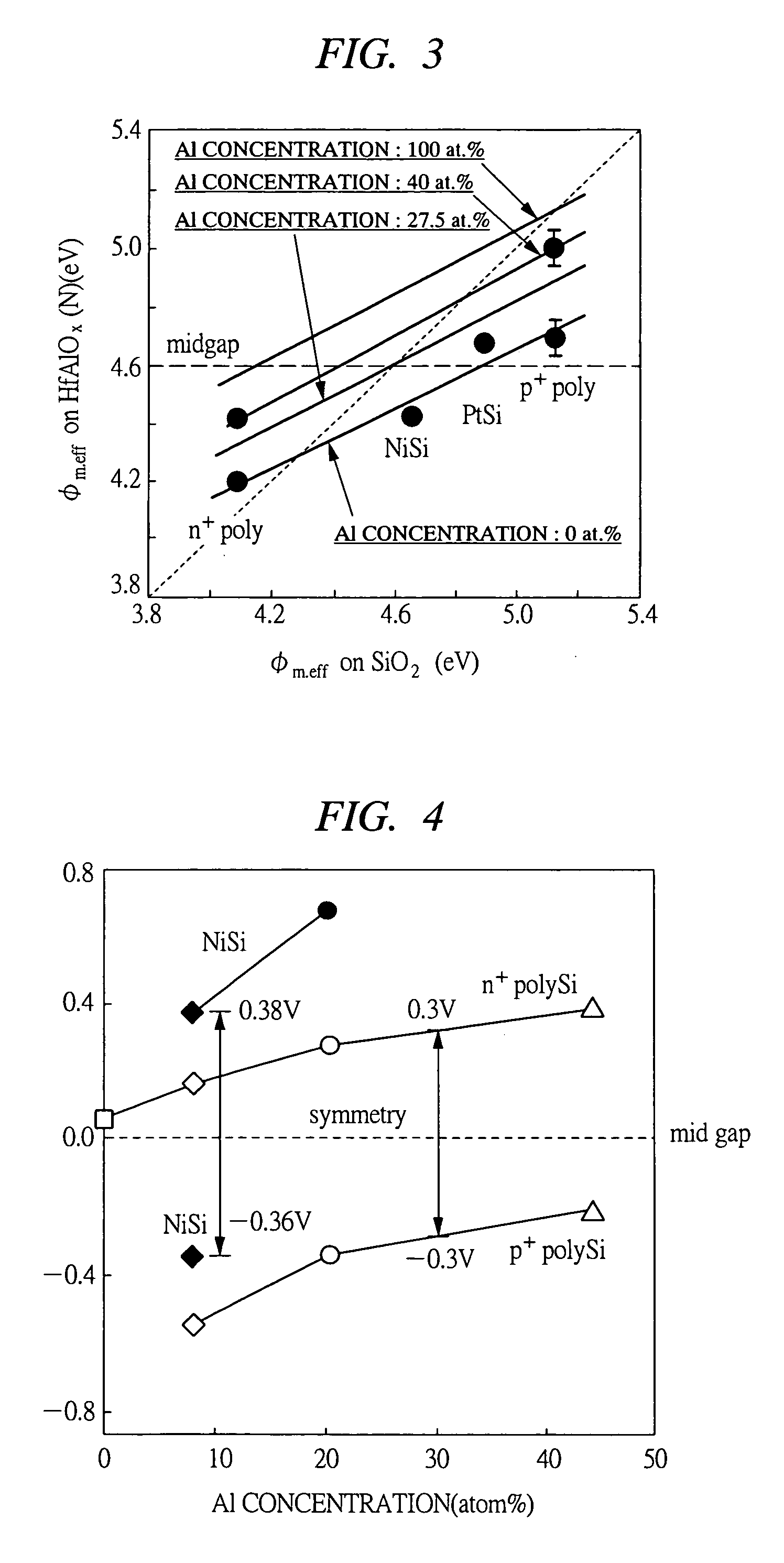
[0057] The feature of the HfAlOx film 5d lies in that the Al concentration in the film is highest at the interface with the gate electrode 6n and it gradually decreases toward the substrate 1. The Al concentration in the film at the interface with the gate electrode 6n and in the vicinity thereof is 20 to 40 atom %, more preferably, 25 to 35 atom % similar to the first embodiment. Also, it is desired that the Al concentration in the HfA...


PUM


Abstract

Threshold voltage of a CMOS transistor which uses a gate insulator made of a hafnium-based high-k material is optimized. A gate insulator of nMOS and pMOS transistors includes a HfOx film and a HfAlOx film formed thereon. At this time, silicon atoms in a n type polycrystalline silicon film which constitutes a gate electrode and Hf atoms in the HfAlOx film are bonded (Hf—Si bonding) and silicon atoms in the n type polycrystalline silicon film and Al atoms in the HfAlOx film are bonded (Al—O—Si bonding) at the interface between the HfAlOx film and the gate electrode. Consequently, the work function of the n type polycrystalline silicon and the work function of the p type polycrystalline silicon are controlled so as to be symmetrical with respect to a midgap (threshold voltage of MOS transistor=0) by changing the Al concentration in the HfAlOx film.

Description

CROSS-REFERENCE TO RELATED APPLICATION [0001] The present application claims priority from Japanese Patent Application No. JP 2005-090591 filed on Mar. 28, 2005, the content of which is hereby incorporated by reference into this application. TECHNICAL FIELD OF THE INVENTION [0002] The present invention relates to a semiconductor device and a manufacturing technology thereof. More particularly, it relates to a technology effectively applied to a semiconductor device having a CMOS transistor in which a gate insulator made of a hafnium-based high-k material is used. BACKGROUND OF THE INVENTION [0003] Conventionally, in a n channel MOS transistor (hereinafter, referred to as a nMOS transistor) and a p channel MOS transistor (hereinafter, referred to as a pMOS transistor) which constitute a CMOS (Complementary Metal Oxide Semiconductor) circuit, a silicon oxide film has been used as a material of a gate insulator, and a polycrystalline silicon film or a polycide film in which a metal sil...

Claims


Application Information

Patent Timeline
IPC IPC(8): H01L29/94
CPCH01L21/823842H01L21/823857
Inventor NABATAME, TOSHIHIDEKADOSHIMA, MASARU
Owner RENESAS TECH CORP
Why Eureka
Try Eureka