Semiconductor laser device

Inactive Publication Date: 2005-07-19
HAMAMATSU PHOTONICS KK
View PDF7 Cites 2 Cited by
  • Summary
  • Abstract
  • Description
  • Claims
  • Application Information

AI Technical Summary

Benefits of technology

[0008]More specifically, this semiconductor laser device is constituted by comprising: a semiconductor laser element; a metal base; and a heat sink interposed between the semiconductor laser element and the metal base, wherein a first metallic layer to increase the adhesiveness of the gold and the semiconductor laser element, and a first Au layer on the upper surface thereof are provided on the surface of the semiconductor laser element on which the active layer is formed. A second metallic layer to increase the adhesiveness of the gold and the heat sink and prevent eutectic bonding, and a second Au layer on the upper surface thereof are provided on the heat sink. The surface of the semiconductor laser element on which the first Au layer is provided and the surface of the heat sink on which the second Au layer is provided are directly joined, and the surface of the heat sink opposing the surface to which the semiconductor laser element is directly joined is attached to the metal base with the conductive adhesive.
[0009]In this way, since the semiconductor laser element and the heat sink are directly joined, the resonator surface of the semiconductor laser does not become contaminated. Further, since the resonator surface does not become contaminated, the surface of the semiconductor laser element on which the active layer is formed and the heat sink can be directly joined. Accordingly, since the semiconductor laser element and the heat sink are joined with good adhesiveness, the heat from the active layer can be effectively radiated directly to the silicon submount.
[0010]Further, the semiconductor laser device according to the present invention is constituted by comprising: a semiconductor laser element; a metal base; and a heat sink interposed between the semiconductor laser element and the metal base, wherein a first metallic layer to increase the adhesiveness of the gold and the semiconductor laser element, and a first Au layer on the upper surface thereof are provided on the surface of the semiconductor laser element on which the active layer is formed. A second metallic layer to increase the adhesiveness of the gold and the heat sink and prevent eutectic bonding, and a second Au layer on the upper

Problems solved by technology

However, the semiconductor laser device shown in FIG. 4 has problems associated with it, such as the conductive adhesive 40 entering the resonator surface of the active layer 12, or adhering thereto during attachment, and this contaminates the resonator surface and produces a defective product.
The problem also arises that a sufficient radiation effect cannot be

Method used


Image

  • Semiconductor laser device
  • Semiconductor laser device
  • Semiconductor laser device

Examples


first embodiment

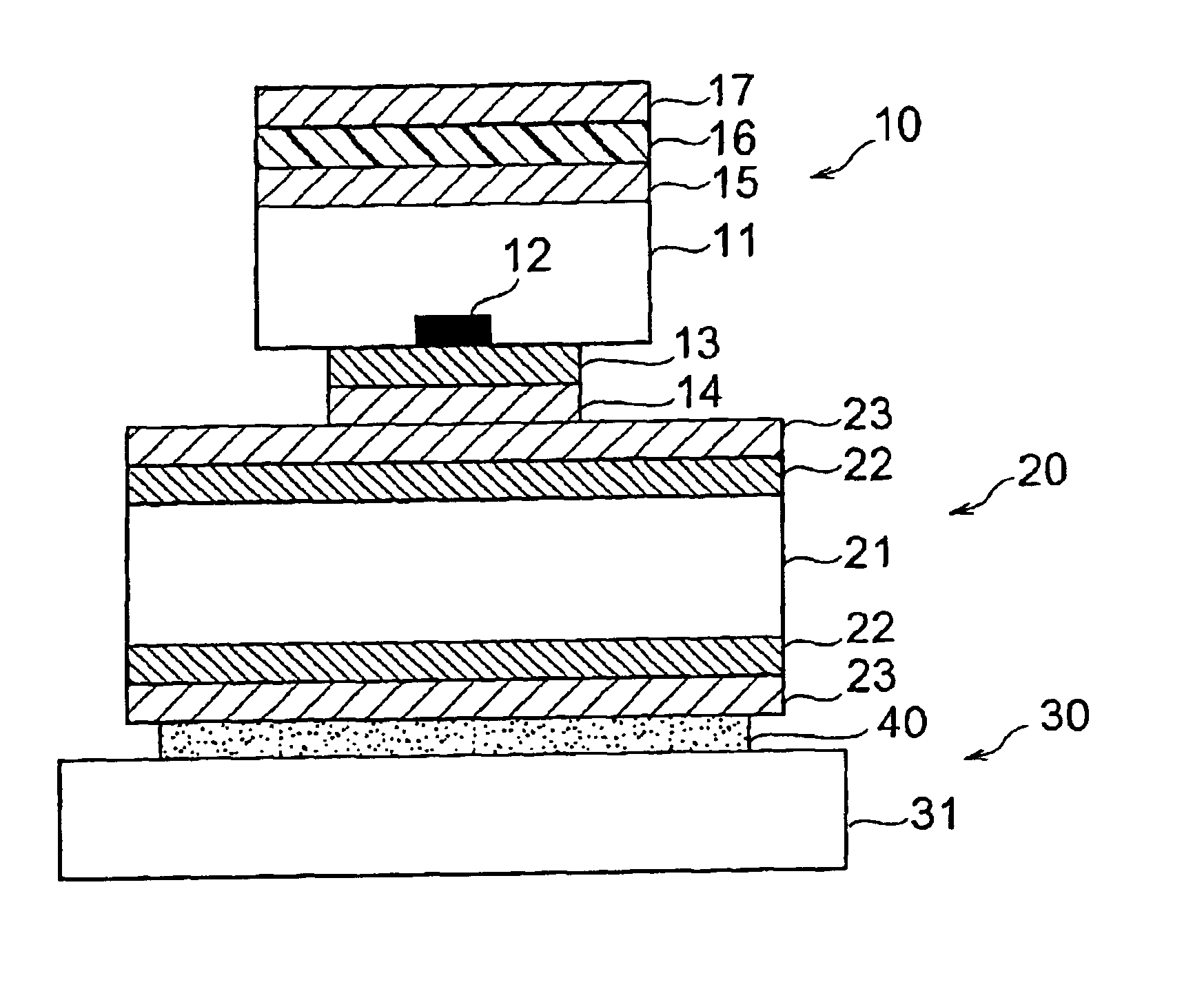
[0022]The Au layer 14 of the semiconductor laser element 10 and the Au layer 23 of the silicon submount 20 are directly joined, and the Au layer 23 of the silicon submount 20 and the metal block 31 of the metal base 30 are attached by a conductive adhesive 40 made of copper solder, and the semiconductor laser device is thereby constituted.

[0023]According to the construction of the semiconductor laser device of the first embodiment shown in FIG. 1, since the semiconductor laser element 10 and the silicon submount 20 are directly joined, the resonator surface of the active layer 12 does not become contaminated, and it is difficult to produce a defective product, so a good yield can be produced. Note that with regard to the active layer 12, the longitudinal direction of the resonator is at right angles to the thickness direction of the semiconductor laser element 10, and laser light is outputted from the end surface (resonator surface) in the longitudinal direction.

[0024]In the semico...

second embodiment

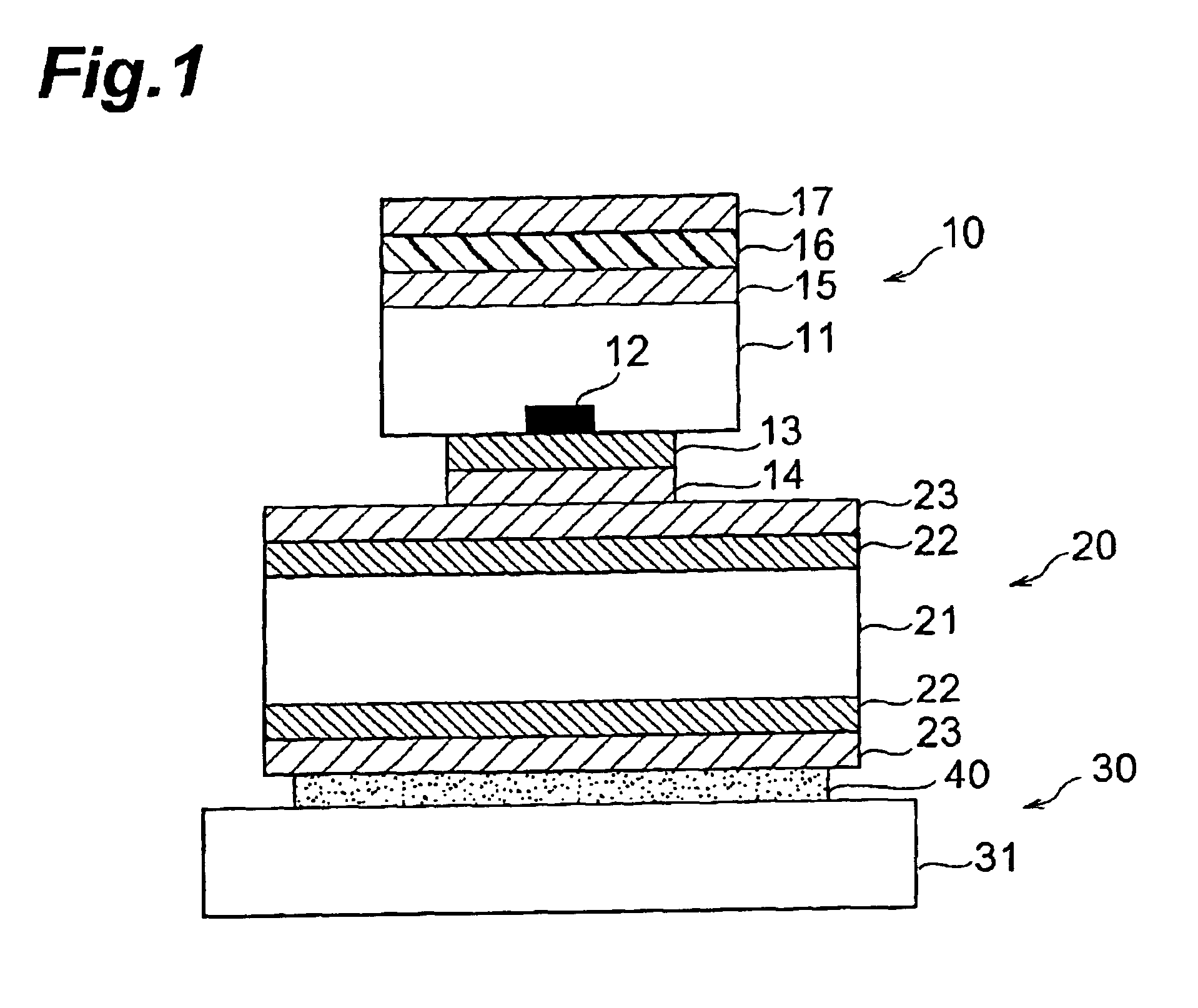
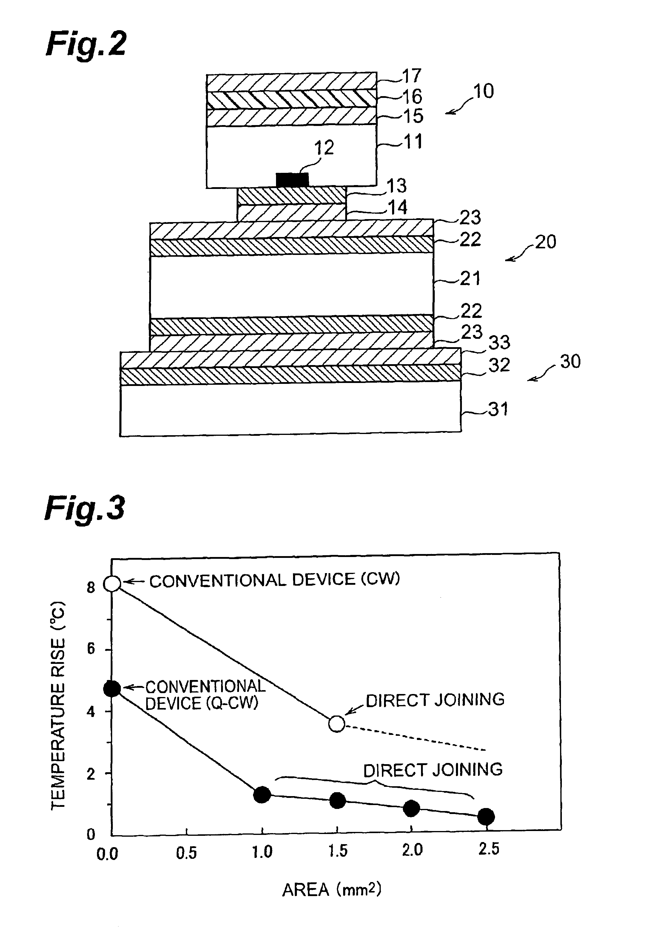
[0026]FIG. 2 is a sectional view of a semiconductor laser device according to the

[0027]The semiconductor laser device according to this embodiment comprises a semiconductor laser element 10, a silicon submount 20, and a metal base 30.

[0028]The semiconductor laser element 10 has an LD 11 containing an active layer 12 made of GaAs, a Cr (metallic) layer 13 with a film thickness of 10 to 30 nm, an electrode made of an Au layer 14 with a film thickness of 300 to 1000 nm, an Au layer 15 with a film thickness of 10 nm, an Au—Ge layer 16 with a film thickness of 250 nm, and an electrode made of an Au layer 17 with a film thickness of 750 nm.

[0029]The silicon submount 20 has a P-type silicon layer 21 as a heat sink, a Cr (metallic) layer 22 with a film thickness of 10 to 30 nm, and an Au layer 23 with a film thickness of 300 to 1000 nm. The metal base 30 has a metal block 31 made of Cu, a Cr (metallic) layer 32, and an Au layer 33.

[0030]The Au layer 14 of the semiconductor laser element 10,...


PUM


Abstract

This semiconductor laser device comprises a semiconductor laser element 10, which is provided with a Cr layer 13 and an Au layer 14, a silicon submount 20, which is provided with a Cr layer 22 and an Au layer 23, and a metal base 30. The surface of the semiconductor laser element 10 on which the Au layer 14 is provided and the surface of the silicon submount 20 on which the Au layer 23 is provided are directly joined together.

Description

TECHNICAL FIELD[0001]The present invention relates to a semiconductor laser device, and particularly to the construction of a semiconductor laser device for radiating heat from an active layer.BACKGROUND ART[0002]FIG. 4 is a longitudinal sectional view of a conventional semiconductor laser device. Reference numeral 10 is a semiconductor laser element, reference numeral 11 is an LD (laser diode), reference numeral 12 is an active layer, reference numeral 13 is a Cr layer, reference numeral 14 is an Au layer, reference numeral 15 is an Au layer, reference numeral 16 is an Au—Ge layer, reference numeral 17 is an Au layer, reference numeral 30 is a metal base, reference numeral 31 is a metal block, and reference numeral 40 is a conductive adhesive. In order to radiate the heat that is generated in the active layer 12, the semiconductor laser element 10 is attached to the metal base 30 by the conductive adhesive 40. The metal base 30 functions as a heat sink.[0003]FIG. 5 is a longitudina...

Claims


Application Information

Patent Timeline
IPC IPC(8): H01S5/02H01S5/00H01S5/022H01S5/042
CPCH01S5/02272H01S5/0224H01S5/0425H01S5/02476H01L24/32H01L2924/12042H01L2924/14H01S5/04252H01S5/0234H01S5/0237H01L2924/00H01S5/024
Inventor SAITOH, MASAYUKIKAN, HIROFUMI
Owner HAMAMATSU PHOTONICS KK
Why Eureka
Try Eureka