Liquid crystal display device and manufacturing method thereof

Active Publication Date: 2012-03-08
HITACHI DISPLAYS +1
View PDF1 Cites 14 Cited by
  • Summary
  • Abstract
  • Description
  • Claims
  • Application Information

AI Technical Summary

Benefits of technology

[0013]An advantage of the present invention is to increase the adhesiveness between the counter electrode and the interlayer insulating film to prevent peeling of the interlayer insulating film from the counter electrode.
[0014]A liquid crystal display device includes: a TFT substrate having a thin-film transistor (TFT) thereon; an organic passivation film disposed so that the organic passivation film covers the TFT; a flat, solid first electrode disposed on the organic passivation film and composed of a transparent conductive film; an interlayer insulating film disposed on the first electrode; a comb-shaped second electrode disposed on the interlayer insulating film and composed of a transparent conductive film; a counter substrate; a color filter disposed beneath the counter substrate; and a liquid crystal layer interposed between the TFT substrate and the counter substrate. An upper portion of the organic passivation film is located be

Problems solved by technology

On the other hand, they have a problem with the viewing angle characteristics.
On the other hand, formation of the interlayer insulating film by low-temperature CVD reduces the adhesiveness of the interlayer insulating film to the counter electrode formed therebeneath.
If the film is peeled during the rubbing process, the peeled film act

Method used


Image

  • Liquid crystal display device and manufacturing method thereof
  • Liquid crystal display device and manufacturing method thereof
  • Liquid crystal display device and manufacturing method thereof

Examples


first embodiment

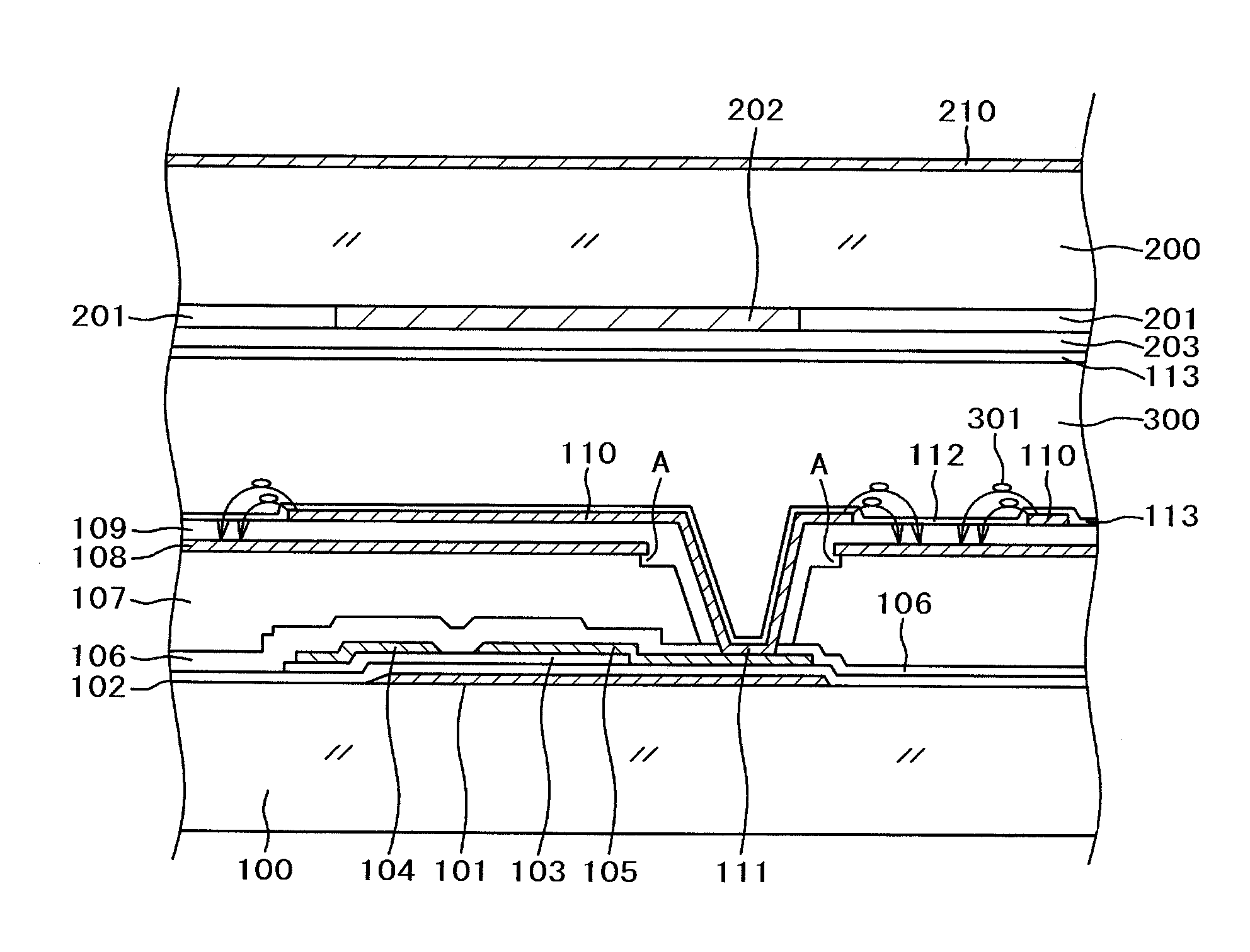
[0026]FIG. 1 is a sectional view showing the structure of the display area of a liquid crystal display device.

[0027]Various types of electrode structures have been proposed and commercialized for IPS-type liquid crystal display devices. The structure shown in FIG. 1 is a currently being used widely. Simply put, a comb-shaped pixel electrode 110 is disposed above a flat, solid counter electrode 108 with an insulating film therebetween. Rotation of liquid crystal molecules 301 using the voltage between the pixel electrode 110 and the counter electrode 108 controls the transmittance of light through a liquid crystal layer 300 for each pixel. Thus, an image is formed. Hereafter, the structure shown in FIG. 1 will be described in detail. While the present invention is described using the structure shown in FIG. 1 as an example, the invention is also applicable in exactly the same way to an IPS type where a comb-shaped counter electrode 108 is disposed above a flat, solid pixel electrode ...


PUM


Abstract

A flat, solid counter electrode is formed on an organic passivation film. Before forming an interlayer insulating film on the counter electrode, plasma ashing is performed. A surface of the organic passivation film is trimmed by the plasma ashing, forming an overhang. The plasma ashing not only trims a surface of the organic passivation film but also roughens a surface of the counter electrode. This increases a contact area between the interlayer insulating film and the organic passivation film or counter electrode, increasing the adhesiveness therebetween. Further, the plasma ashing eliminates the remainder of a resist on the counter electrode, increasing the adhesiveness of the interlayer insulating film.

Description

CLAIM OF PRIORITY[0001]The present application claims priority from[0002]Japanese Patent Application JP 2010-197325 filed on Sep. 3, 2010, the content of which is hereby incorporated by reference into this application.FIELD OF THE INVENTION[0003]The present invention relates to a display device and in particular to an in-plane switching (IPS) liquid crystal display device which has improved reliability by preventing peeling of a film between layers.BACKGROUND OF THE INVENTION[0004]Liquid crystal display devices include a TFT substrate having a pixel electrode, a thin-film transistor (TFT), and the like arranged in a matrix thereon; a counter substrate disposed so that it is opposed to the TFT substrate and having a color filter and the like disposed in positions corresponding to the pixel electrode on the TFT substrate therebeneath; and liquid crystal interposed between the TFT substrate and the counter substrate. Liquid crystal display devices form an image by controlling the trans...

Claims


Application Information

Patent Timeline
IPC IPC(8): G02F1/1335H01L33/42
CPCG02F1/136227G02F1/134363
Inventor ISHIGURO, KEISUKESHINOKI, YOICHI
Owner HITACHI DISPLAYS
Why Eureka
Try Eureka