

Optical component, infrared camera, and method for manufacturing optical component
- Summary
- Abstract
- Description
- Claims
- Application Information
AI Technical Summary
Benefits of technology
Problems solved by technology
Method used
Image


Examples
example 1
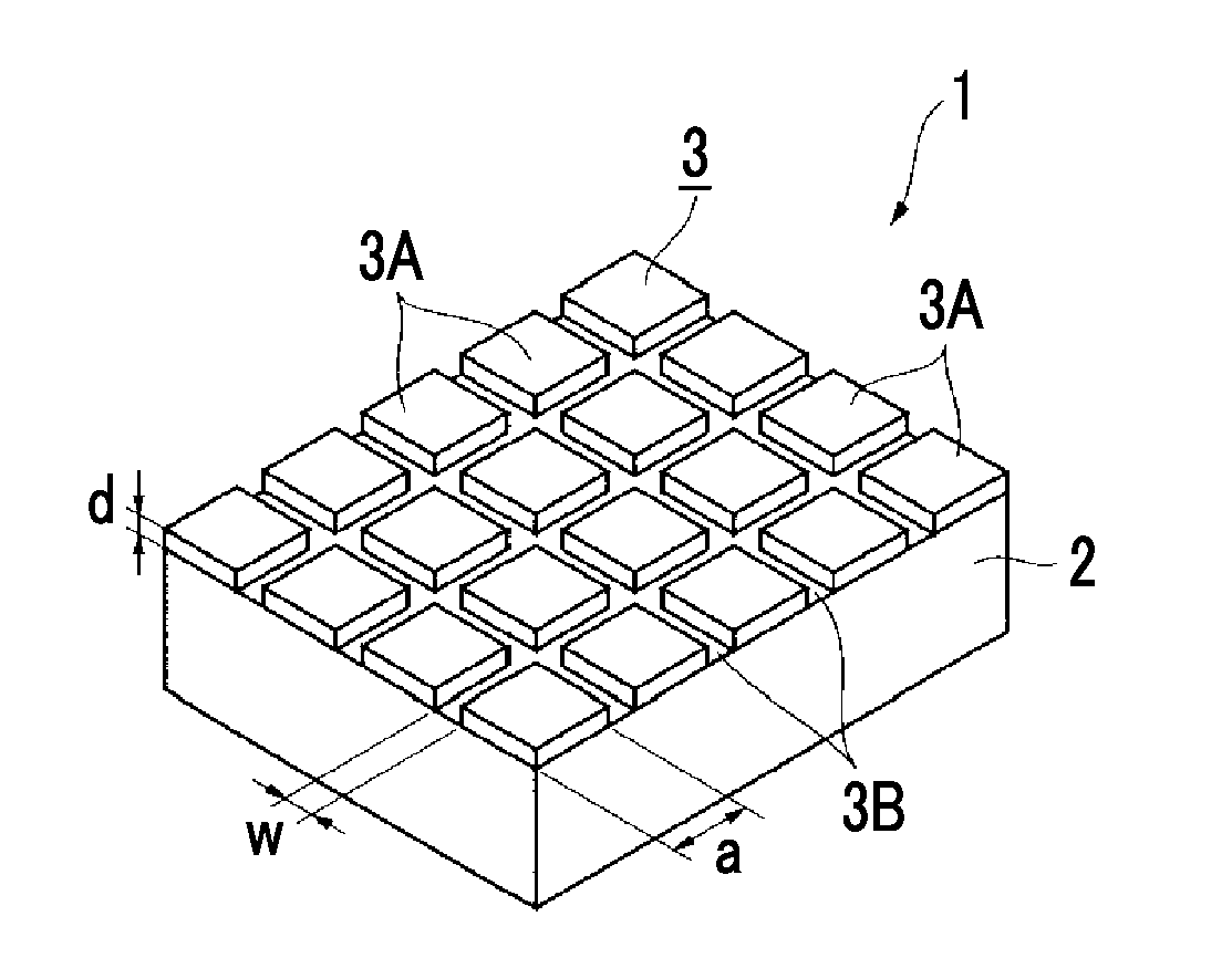
[0054]In the conditions described below, an antireflection film is formed by using the first manufacturing method so as to produce a sample of an optical component.
[0055]
[0056]Antireflection materials obtained by mixing carbon particles (obtained by grinding C film of which an average particle diameter is 0.3 μm) with olefin-based UV curing resins were used. In this antireflection material, a refractive index to light having a wavelength of 10.5 μm was 2.6. The surface tension of this antireflection material was 30 mN / m, and the viscosity was 20 cps.
[0057]
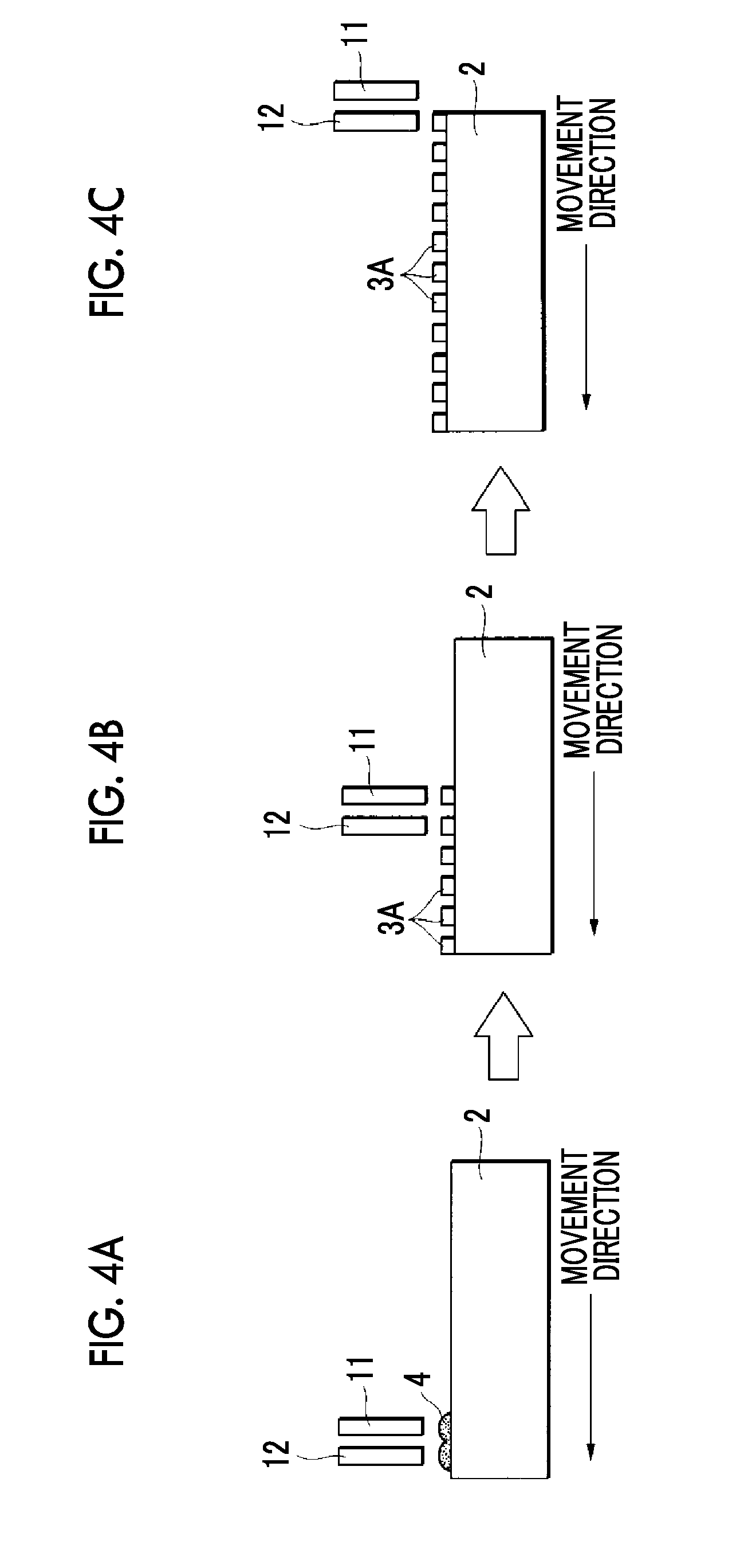
[0058]An IJ head (Model No. PN700-10701-01) manufactured by Dimatix, Inc. was used as an ink jet coating device. A nozzle diameter of this device was 20 and a discharge amount was 15 pliters / time. In this example, discharging and curing of the ultraviolet ray cured resin were performed for three times, so as to form an antireflection film consisting of a dot-shaped antireflection material. Here, as the ultraviolet rays (UV) for cur...
example 2
[0099]According to the conditions described below, a sample of an optical component was produced by forming an antireflection film by using the second manufacturing method.
[0100]
[0101]Antireflection materials obtained by mixing carbon particles (obtained by grinding diamond like carbon film of which an average particle diameter is 0.3 μm) with olefin-based UV curing resins were used. In this antireflection material, a refractive index to light having a wavelength of 10.5 μm was 2.6. The surface tension of this antireflection material was 30 mN / m, and the viscosity was 20 cps.
[0102]
[0103]An IJ head (Model No. PN700-10701-01) manufactured by Dimatix, Inc. was used as an ink jet coating device. A nozzle diameter of this device was 20and a discharge amount was 15 pliters / time. In this example, discharging and curing of the ultraviolet ray cured resin were performed for three times, so as to form an antireflection film consisting of dot-shaped antireflection materials. Here, as the ultra...
PUM
| Property | Measurement | Unit |
|---|---|---|
| Length | aaaaa | aaaaa |
| Length | aaaaa | aaaaa |
| Length | aaaaa | aaaaa |
Abstract
Description
Claims
Application Information