

Methods for the electronic, homogeneous assembly and fabrication of devices
a technology of homogeneous assembly and electronic components, applied in the direction of digital storage, record information storage, flat carrier supports, etc., can solve the problems of increasing cost of conventional integration techniques, and achieve the effect of reducing the number of electrodes on the motherboard and simplifying the devi
- Summary
- Abstract
- Description
- Claims
- Application Information
AI Technical Summary
Benefits of technology
Problems solved by technology
Method used
Image

Examples
Embodiment Construction
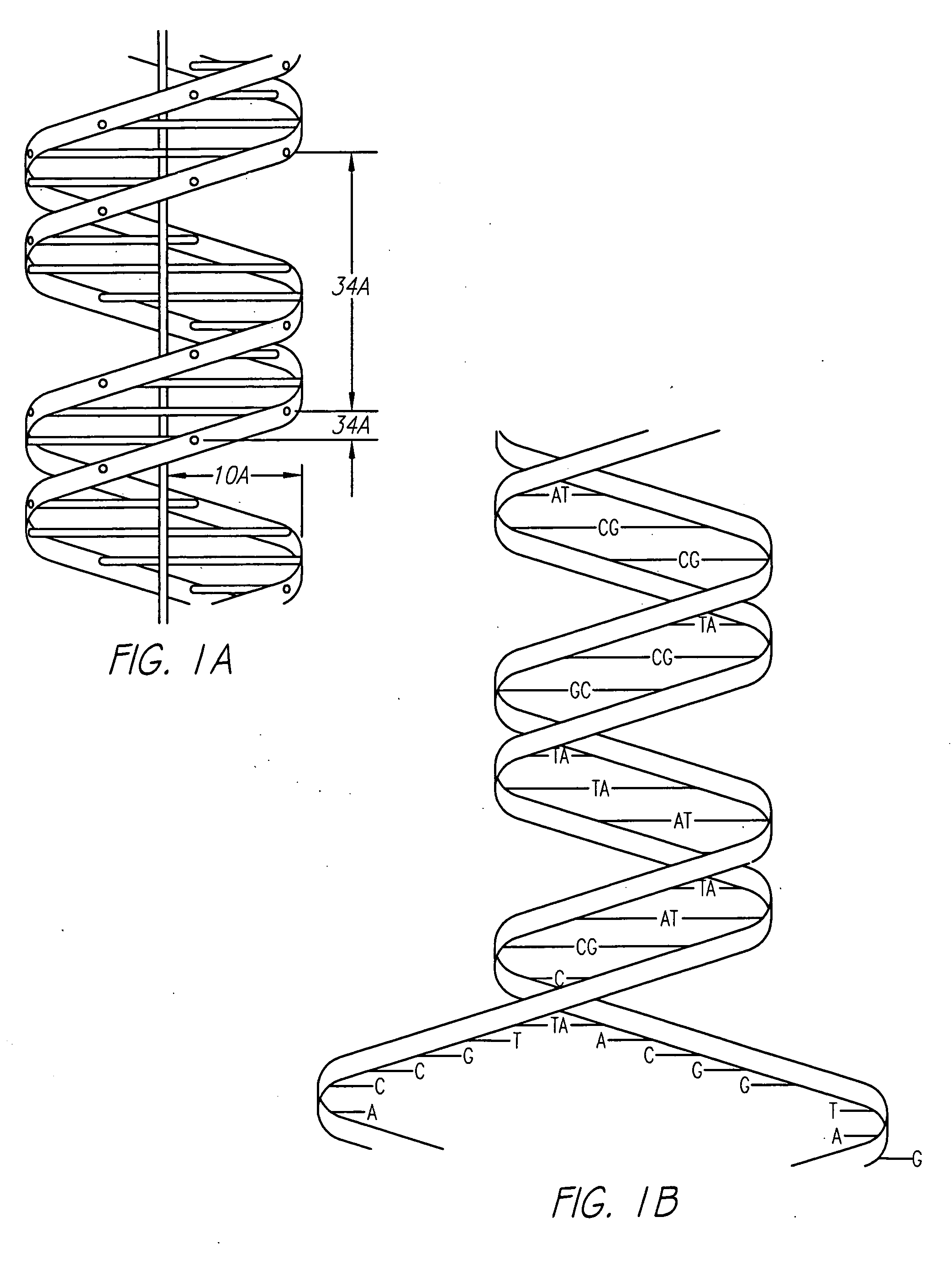
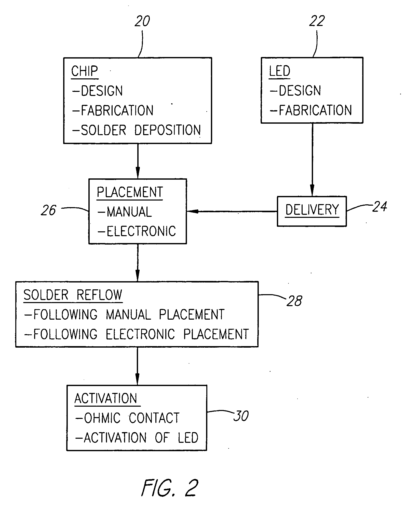
[0081]FIG. 2 is a flow chart showing major components typically included in implementation of these inventions. At one level of generality, the inventions utilize the combination of fluidics and electronics for the transport and placement of a component device on a target device (sometimes referred to as a motherboard). Various modes of transport utilizing electronics, typically in a medium, most typically a fluid medium, include electrophoretic transport, electroosmotic transport, and dielectrophoretic action, including orientation and transport. Electrostatic potentials may be utilized with or without the presence of fluid. Electroosmotic transport is typically considered to be surface phenomenon, and accordingly, such transport is typically found close to the surface, most typically a charged surface, which results in a net fluid flow.
[0082]FIG. 2 identifies two primary components, a chip or motherboard 20 and a component device 22. Typically, the chip or motherboard 20 will inc...
PUM
| Property | Measurement | Unit |
|---|---|---|
| size | aaaaa | aaaaa |
| diameter | aaaaa | aaaaa |
| lengths | aaaaa | aaaaa |
Abstract
Description
Claims
Application Information