Embedded IC test circuits and methods

a technology of embedded ic and test circuit, applied in the direction of transmitter monitoring, gated amplifier, transmitter monitoring, etc., can solve the problems of manufacturing new, ever more complex integrated circuits

Inactive Publication Date: 2006-09-28
UNIV OF FLORIDA RES FOUNDATION INC
View PDF16 Cites 31 Cited by
  • Summary
  • Abstract
  • Description
  • Claims
  • Application Information

AI Technical Summary

Problems solved by technology

This is largely due to the fact that in most instances the expenses associated with complex testing equipment and time lost in testing are among the more significant factors contributing to the costs of designing and manufacturing new, ever more complex integrated circuits (ICs).

Method used


Image

  • Embedded IC test circuits and methods
  • Embedded IC test circuits and methods
  • Embedded IC test circuits and methods

Examples


Embodiment Construction

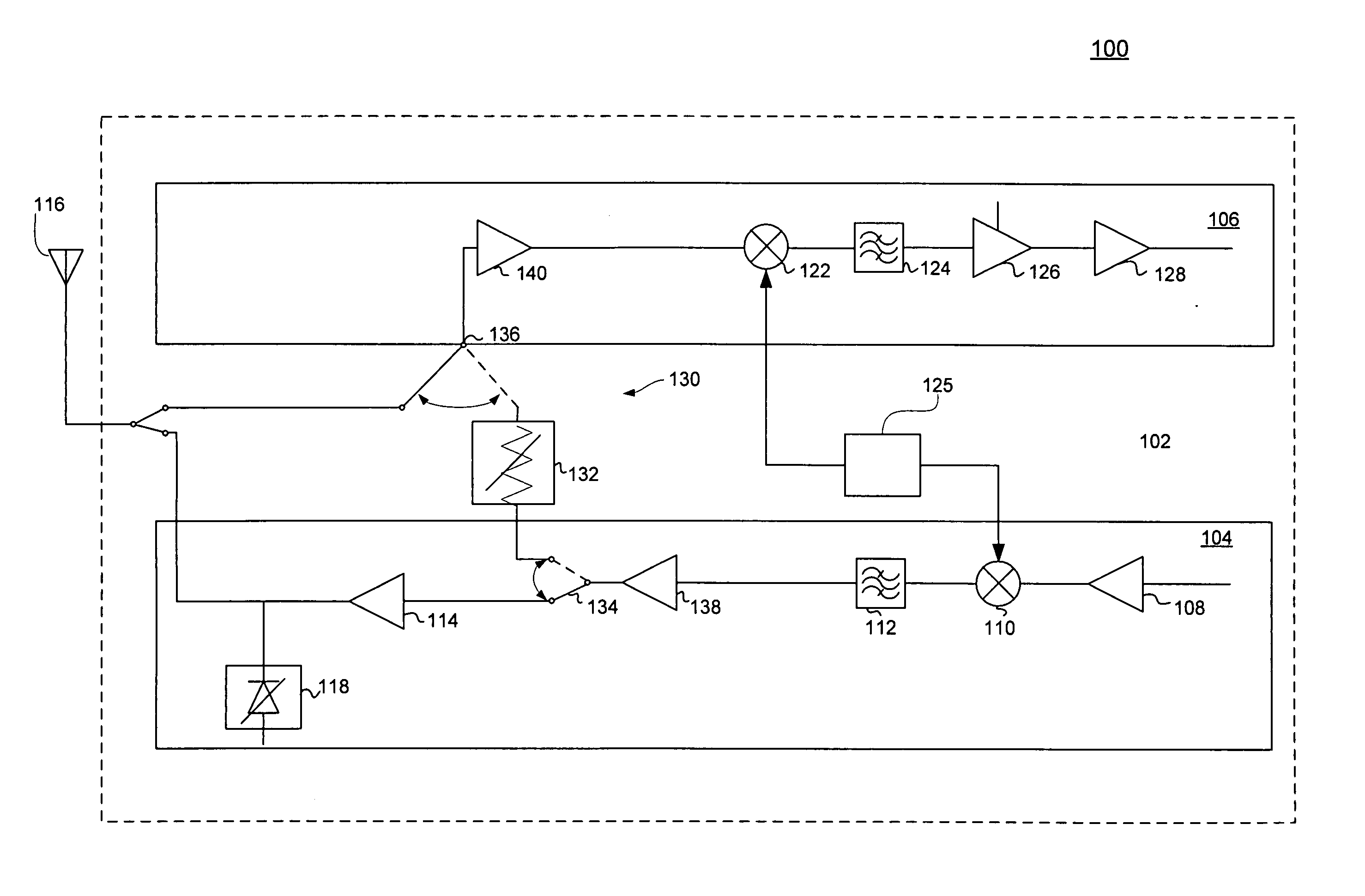
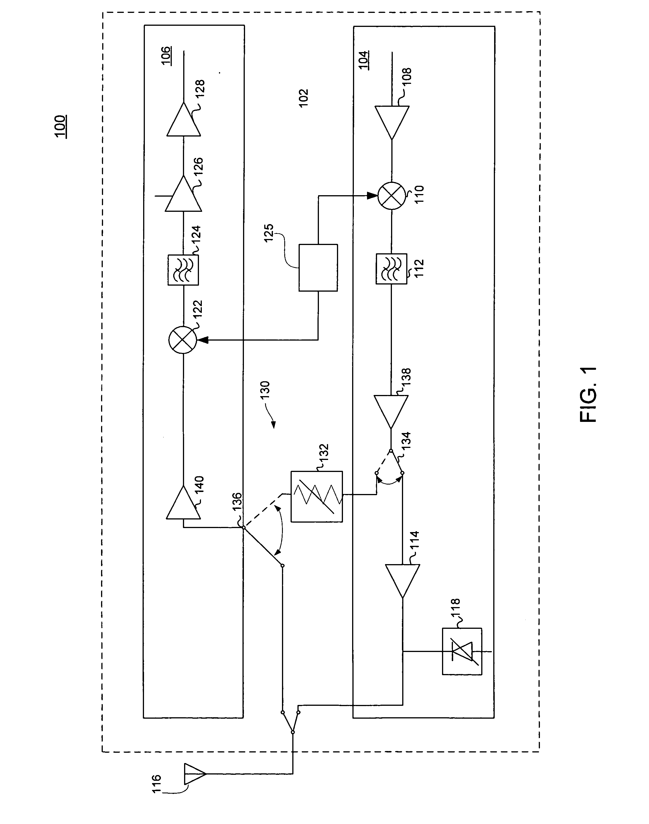
[0020]FIG. 1 provides a schematic diagram of a self-testing transceiver 100, according to one embodiment of the invention. The self-testing transceiver 100 has an on-chip power detection capability, and, as illustrated, comprises a substrate 102 on which a transmitter 104 and a receiver 106 are disposed. The transmitter 104 illustratively includes an amplifier 108, a first mixer 110 connected to the amplifier, and a first filter 112 connected to the first mixer. As further illustrated, the transmitter 104 also includes a high-power amplifier 114 that electrically connects to an antenna 116 for effecting wireless signal transmissions. The transmitter 104 also illustratively includes a detector 118, which as shown is electrically coupled to the high-power amplifier 114.

[0021] The receiver 106 illustratively includes a second mixer 122 and a second filter 124 connected to the second mixer. Illustratively, a synthesizer 125 is connected between the first mixer 110 and the second mixer ...


PUM


Abstract

A self-testing transceiver having an on-chip power detection capability is provided. The self-testing transceiver can include a semiconductor substrate and a transmitter having a high-power amplifier disposed on the substrate. The self-testing transceiver also can include a receiver disposed on the substrate for selectively coupling to an antenna. The self-testing transceiver can further include at least one power detector disposed on the semiconductor substrate for determining a power such as an RMS and / or peak-power of a signal at an internal node of the self-testing transceiver. Additionally, the self-testing transceiver can include a loopback circuit disposed on the substrate.

Description

BACKGROUND [0001] 1. Field of the Invention [0002] The present invention is related to the field of electronic circuit testing, and, more particularly, embedded testing of electronic circuits. [0003] 2. Description of the Related Art [0004] Electronic circuit designers face a seemingly relentless demand for new electronic devices that can provide increasingly sophisticated capabilities and offer ever greater bandwidth operability. This demand is reflected in the drive to integrate various digital and analog components in smaller areas, using fewer chips. Indeed, a frequently-cited goal is to create an integrated system on a single chip, a so-called “system-on-a-chip” (SoC) in which a small crystal of silicon or other semiconductor material would be fabricated to carry out each of the various electronic functions of an entire system. Aided by advances in processing technologies, electronic circuit designers are moving ever closer to this goal by increasingly integrating various digit...

Claims


Application Information

Patent Timeline
Patent Type & Authority Applications(United States)
IPC IPC(8): H01Q11/12
CPCH03F3/24H03F3/50H03F3/72H04B17/318H03F2203/5031H04B2001/0408H04B17/19H03F2200/105
Inventor EISENSTADT, WILLIAM R.FOX, ROBERT M.YOON, JANG SUPZHANG, TAO
Owner UNIV OF FLORIDA RES FOUNDATION INC
Why Eureka
Try Eureka