

Hdp-cvd seasoning process for high power hdp-cvd gapfil to improve particle performance
a technology of hdpcvd and seasoning process, which is applied in the direction of coating, chemical vapor deposition coating, semiconductor devices, etc., can solve the problems of damage to the chamber, adversely affecting the yield of wafers, and unwanted deposition on the walls
- Summary
- Abstract
- Description
- Claims
- Application Information
AI Technical Summary
Benefits of technology
Problems solved by technology
Method used
Image

Examples
examples
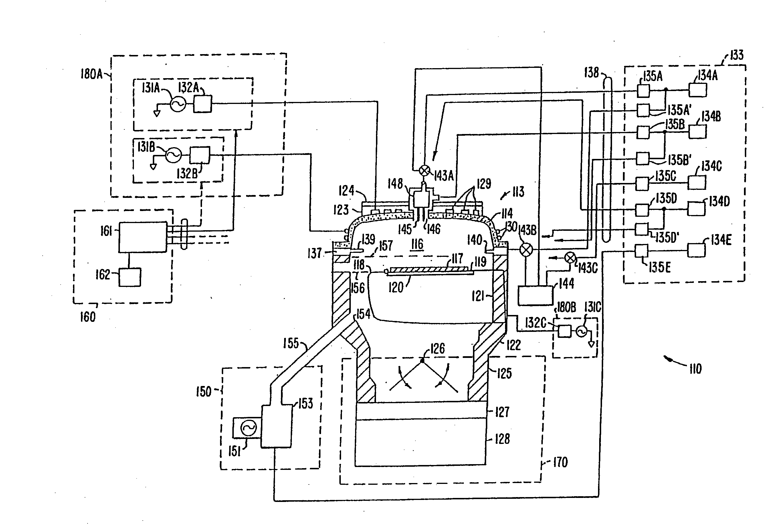
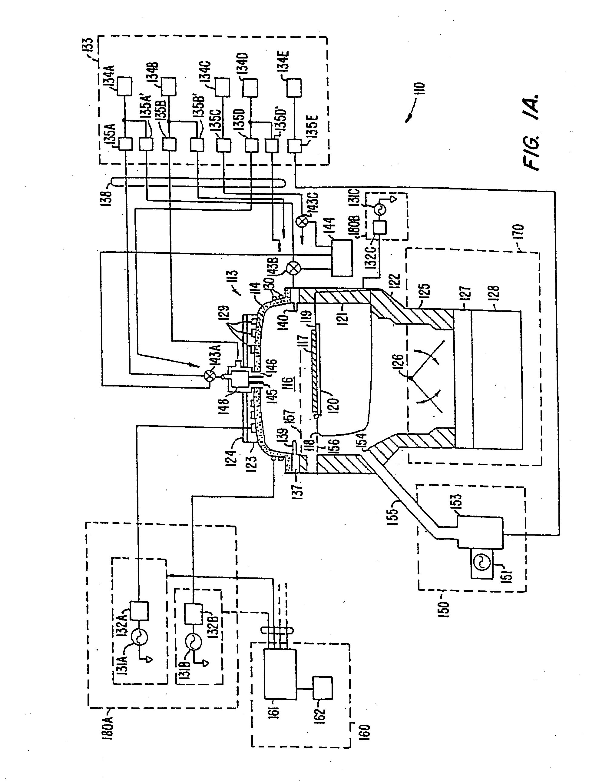
[0068] Examples will now be described of forming and testing seasoning films according to embodiments of the invention. In Example 1, a comparison is made of the number of particles added to a substrate from a conventional seasoning film and seasoning films according to embodiments of the invention. Particles from the seasoning film (referred to as particle adders) greater than 0.20 micrometers were counted on 200 mm substrate wafers after a heating process was performed The heating process includes striking and maintaining a plasma for 45 to 60 seconds with an RF power of about 4800 watts. The plasma is formed from oxygen (O2) and argon.
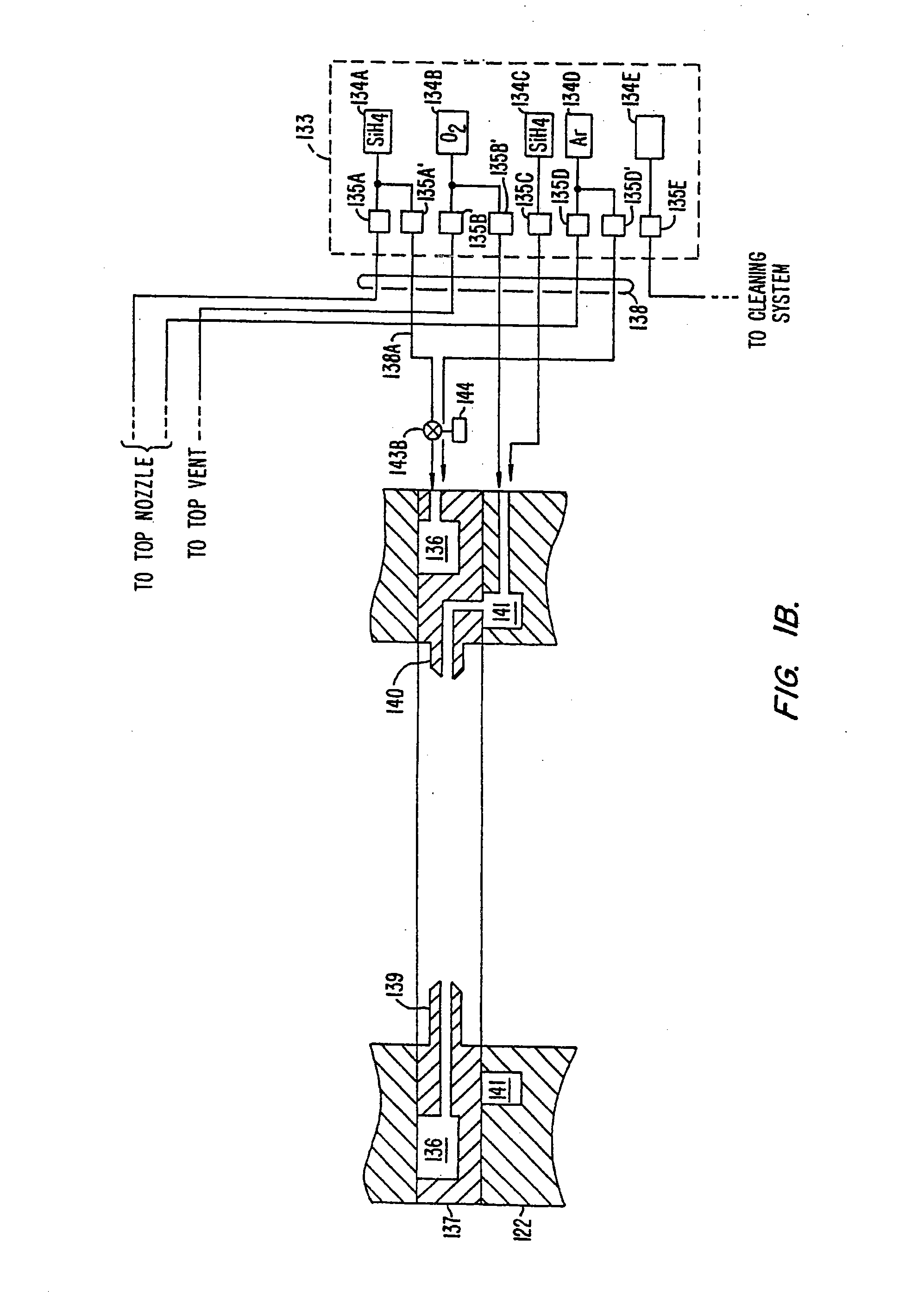
[0069] The conventional seasoning film was formed on inside surfaces of an ULTIMA™ chamber (including aluminum nitride nozzles) through a conventional film forming process. This process included flowing 290 sccm of oxygen (O2), 180 sccm of silane (SiH4), and 110 sccm of argon into the chamber from aluminum nitride nozzles positioned on the sides of...
PUM
| Property | Measurement | Unit |
|---|---|---|
| feature sizes | aaaaa | aaaaa |
| diameter | aaaaa | aaaaa |
| diameter | aaaaa | aaaaa |
Abstract
Description
Claims
Application Information