

Fabrication of long range periodic nanostructures in transparent or semitransparent dielectrics
a technology of semi-transparent dielectrics and periodic nanostructures, applied in the field of nanotechnology, can solve problems such as grating formation, and achieve the effect of relieving build-up stress
- Summary
- Abstract
- Description
- Claims
- Application Information
AI Technical Summary
Benefits of technology
Problems solved by technology
Method used
Image

Examples
Embodiment Construction
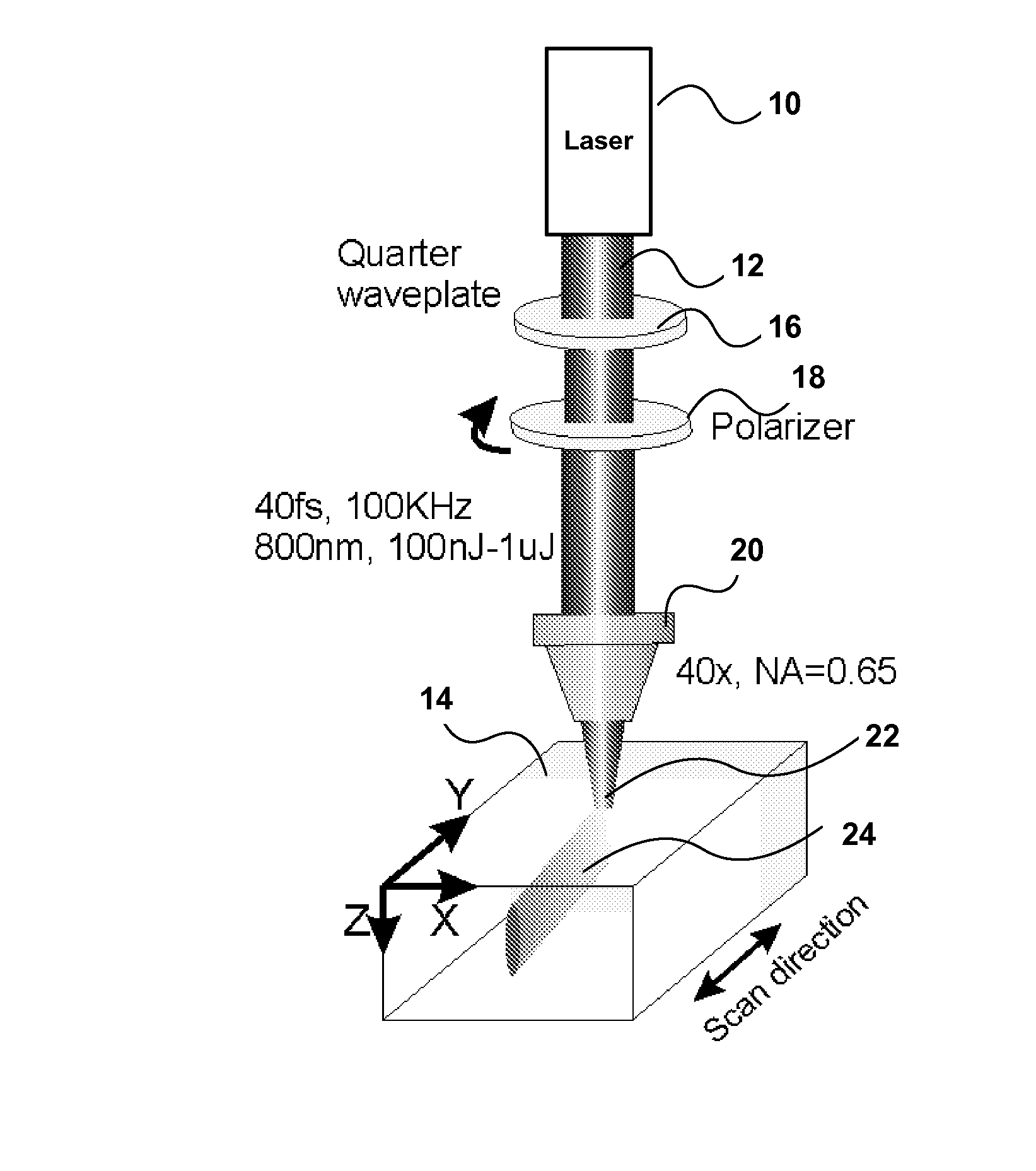
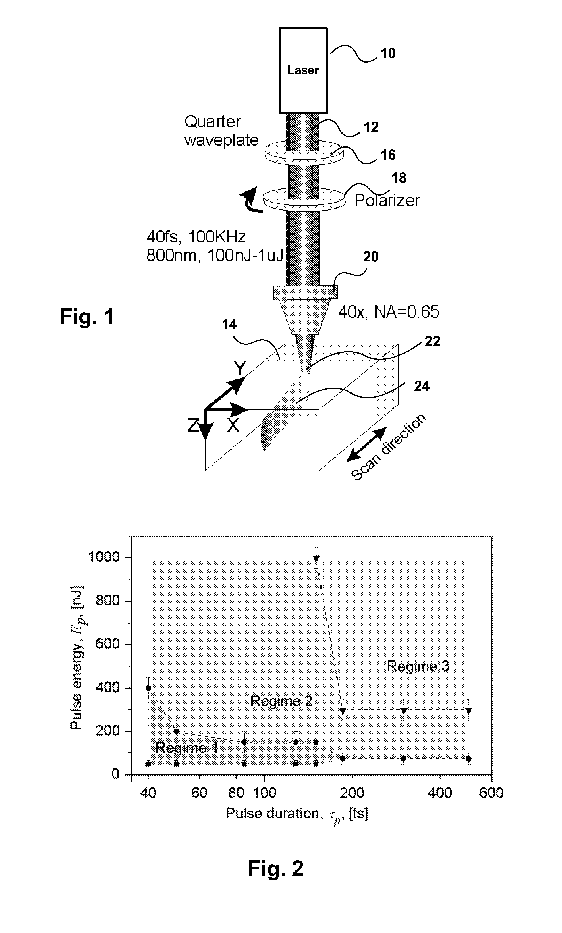
[0036] An apparatus for producing high quality long-range periodic sub-diffraction limit nanostructures using FLDM in accordance with one embodiment of the invention is shown in FIG. 1. This apparatus comprises a Ti:sapphire near-infrared femtosecond laser 10 generating laser beam 12, which is directed onto a transparent substrate 14 of fused silica. Other configurations for laser writing such as longitudinal excitation (scan direction is parallel to the light propagation direction) can also be used. It is also possible to overlap consecutive writing beams to create a wider region of grating-like slabs. As mentioned previously the degree of overlap should be approximately 50-70% of the width of the original laser written single-pass modified region. Such overlap is necessary so that the sub-wavelength periodicity of the first laser written modified region is transferred or imposed coherently onto the second laser modified region etc. so that the broader modified region has a single ...
PUM
| Property | Measurement | Unit |
|---|---|---|
| energy | aaaaa | aaaaa |
| temperatures | aaaaa | aaaaa |
| lengths | aaaaa | aaaaa |
Abstract
Description
Claims
Application Information