Process of producing light emitting panel, process of producing display panel and display panel

a technology of light emitting panel and display panel, which is applied in the direction of discharge tube/lamp details, organic semiconductor devices, discharge tubes luminescnet screens, etc., can solve the problems of increasing the production steps of uncured photocurable resin adhesion to organic el display panel, and uncured photocurable resin removal by washing, so as to reduce the number of materials, improve the production yield, and simplify the production step of polyhedral chamfer

Active Publication Date: 2006-10-05
SANYO ELECTRIC CO LTD
View PDF2 Cites 36 Cited by
  • Summary
  • Abstract
  • Description
  • Claims
  • Application Information

AI Technical Summary

Benefits of technology

[0043] Therefore, according the structure of the display panel of the present invention, the organic fluoride compound layer is made to double as the adhesion preventive layer that covers the terminal section to prevent the adhesive on the organic EL element of the display panel from adhering to the terminal and as the material of the charge transport layer or charge injection layer used as the organic EL element. Therefore, it is unnecessary to use a special material as the adhesive element layer covering the terminal section, making it possible to reduce the number of materials.
[0044] According to this invention, a process of producing a light emitting

Problems solved by technology

Therefore, there is such an disadvantage that the steps of producing the organic EL display panel are increased.
Moreover, there is the disadvantage that an uncured photocurable resin adheres to the organic EL display panel when the above display regions are divided.
There is the possibility that such an uncured photocurable resin adheres to various places in the subsequent working steps and therefore, the uncured photocurable resin is removed by washing.
However, in this case, the organic solvent and the li

Method used


Image

  • Process of producing light emitting panel, process of producing display panel and display panel
  • Process of producing light emitting panel, process of producing display panel and display panel
  • Process of producing light emitting panel, process of producing display panel and display panel

Examples


embodiment 1

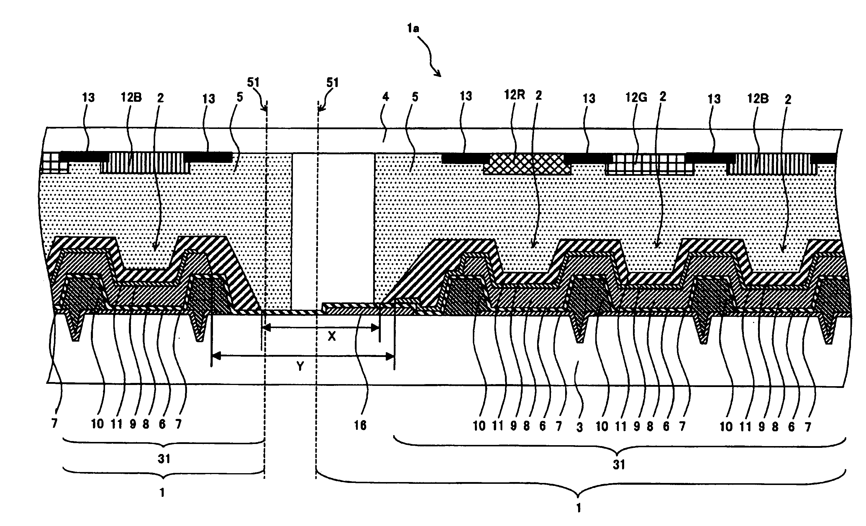
[0051] First, the structure of an organic EL display panel manufactured using a production process according to this embodiment will be explained with reference to FIGS. 1 to 4C.

[0052] 1-1. Whole Structure of the Organic EL Display Panel

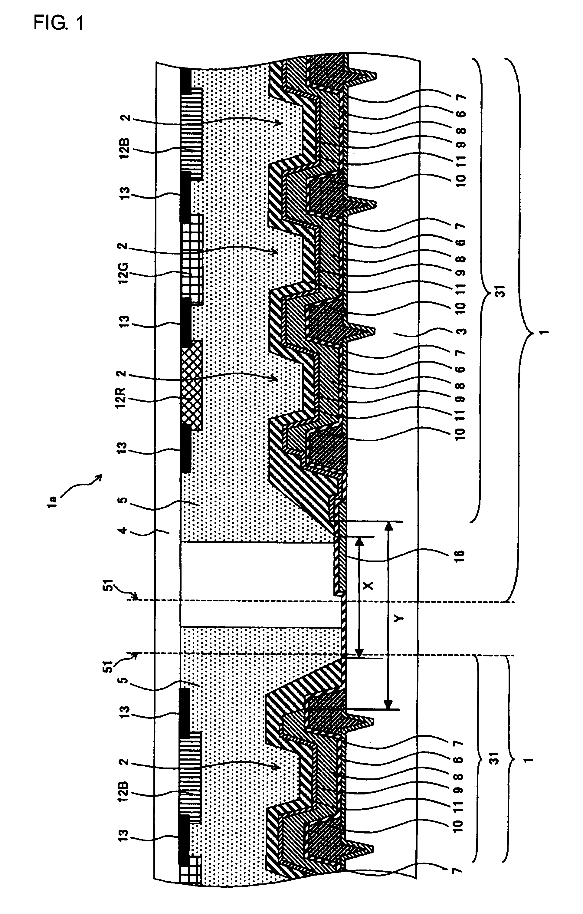
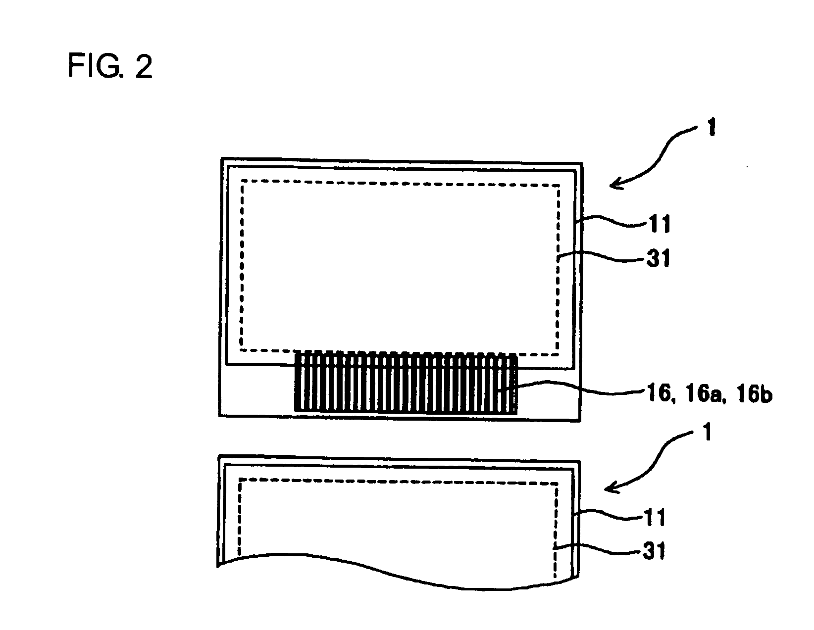
[0053]FIGS. 1 and 2 are a typical sectional view and a plan view for explaining the structure of the organic EL display panel produced using a production process according to this embodiment.

[0054]FIG. 1 shows the state of a laminate 1a before neighboring organic EL display panels 1 are divided into two organic EL display panels and is a view illustrating two organic EL display panels adjacent to each other through a dividing part 51. After the laminate 1a is produced, the neighboring organic EL display panes 1, 1 are divided at the dividing part 51. The organic EL display panel 1 is structured by sealing a display region 31 between a support substrate 3 and a seal plate 4 for sealing through a seal layer 5 for sealing.

[0055] The support substrat...

embodiment 2

[0106] In this embodiment, the above limiting layer 11 is formed, then, the surface of the limiting layer 11 is surface treated by a coupling agent and the support substrate 3 on which the limiting layer 11 is formed is applied to the seal plate 4 coated with the adhesive forming the seal layer 5. The embodiment 2 is the same as the embodiment 1 except for the above process. The adhesive strength between the limiting layer 11 and the seal layer 5 can be improved by the surface treatment using such a coupling agent.

[0107] When the coupling agent has a reacting group that chemically combines with various seal layers 5, it can improve the interfacial strength with the seal layer 5.

[0108] The above surface treatment is carried out as follows: the coupling agent is applied to the side of the support substrate 3 to which side the display region 31 is applied through the seal layer 5 between the support substrate 3 and the seal plate 4 among the surface of the support substrate 3, and af...

example 1

[0117] Examples in which an organic EL display panel 1 is manufactured using the production process of the above embodiment 1 will be shown.

[0118] As shown in FIG. 3A, a terminal section 16 was formed on a support substrate 3 made of a TFT substrate. As the terminal section 16, a Cr film was formed by a sputtering method.

[0119] Also, an anode 7 was formed on an electrode of the TFT substrate 6 and a cell separation film 10 was further formed.

[0120] Next, an adhesion preventive layer 6 was formed on the entire surface of the support substrate 3 (FIG. 3B). As the adhesion preventive layer 6, carbon fluoride (CFX) was formed by a plasma CVD (chemical vapor phase deposition) method using methane trifluoride (CHF3) as raw material gas. The film was formed in the following condition: pressure when the film was formed: 20 Pa, power used to apply bias voltage: 100 W, time for film formation: 10 seconds.

[0121] In succession, as shown in FIG. 3C, an organic film 8 was vapor-deposited on t...


PUM


Abstract

The invention relates to a process of producing a display panel, the process comprising a step of providing plural display regions on the principal plane of a support substrate, a step of applying an adhesive to the principal plane of the support substrate so as to cover the display region, to form a seal layer and laminating a seal plate through the seal layer to form a laminate and a step of dividing the laminate at the positions between the display adjacent to each other to produce plural light emitting panels each having the display region, the process further comprising a step of forming an adhesion preventive layer that inhibits adhesion to the adhesive on the principal plane of the support substrate between the display regions adjacent to each other prior to the application of the adhesive.

Description

BACKGROUND OF THE INVENTION [0001] 1. Field of the Invention [0002] The invention relates to a process of producing plural light emitting panels by sealing plural luminous regions between a support substrate and a seal plate which constitute a unit and by dividing the resulting product. [0003] Also, the invention relates to a process of producing plural display panels by sealing plural display regions between a support substrate and a seal plate which constitute a unit and by dividing the resulting product. [0004] Also, the present invention relates to a display panel. [0005] 2. Description of the Related Art [0006] A remarkable attention has been focused on electroluminescence (hereinafter abbreviated as an organic EL) elements as self-emitting type luminous elements in recent years and organic EL displays using these organic EL elements are being developed. Organic EL elements have the characteristics, such as high response speed and operations carried out under low voltage by low...

Claims


Application Information

Patent Timeline
IPC IPC(8): H01L51/52H01L51/56H01L27/28
CPCH01L27/322H01L27/3244H01L51/0024H01L2251/566H01L51/5246H01L51/56H01L51/5237H10K59/38H10K59/12H10K71/50H10K50/841H10K50/8426H10K71/851H10K71/00
Inventor HARADA, GAKU
Owner SANYO ELECTRIC CO LTD
Why Eureka
Try Eureka