Integrated smart power switch

a smart power switch and integrated technology, applied in the field of semiconductors and systems, can solve the problems of inability to sustain continuous power dissipation associated with linear operation, the effect of non-uniform doping and voids in the die attachment material can produce variations in current density and temperature across the devi

Active Publication Date: 2006-10-05
RAYTHEON CO
View PDF11 Cites 56 Cited by
  • Summary
  • Abstract
  • Description
  • Claims
  • Application Information

AI Technical Summary

Problems solved by technology

A problem associated with a type of power transistors known as a metal oxide semiconductor field effect transistors (MOSFETs), as well as with Insulated Gate Bipolar Transistors (IGBTs) is that they can be optimized as switches and cannot sustain continuous power dissipation associated with operation in the linear mode.
However, non-uniform doping and voids in the die attachment material can produce variations in the current density and temperature across the device.
The higher current causes further gain increase that ultimately results in the thermal runaway and catastrophic failure of the device.
Unfortunately, as switching performance of this device improves, the crossover current increases and its linear operation deteriorates.
However, the FBSOA and RBSOA curves limit only the maximum drain to source voltage ratings.
As a result, many designs can not tolerate changed environmental or circuit conditions such as operating at a higher junction temperature in an emergency with reduced coolant flow or providing higher current to a stalled motor.
However such oversizing still does not prevent the devices from being underused in one mode of operation and overstressed in another.
At present, power transistors suffer from a lack of diagnostics and prognostics wherein it is difficult to determine if anything is wrong with working power semiconductors.
For example, the existing method for predicting power transistor reliability would not account for a device failure caused by overstressed die contact to the substrate or faulty mounting to the heat sink.
Further, no methods of inspecting and calibrating installed transistors according to their power handling capability exist at the present time.

Method used


Image

  • Integrated smart power switch
  • Integrated smart power switch
  • Integrated smart power switch

Examples


Embodiment Construction

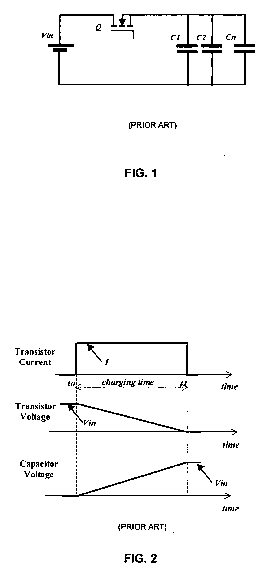
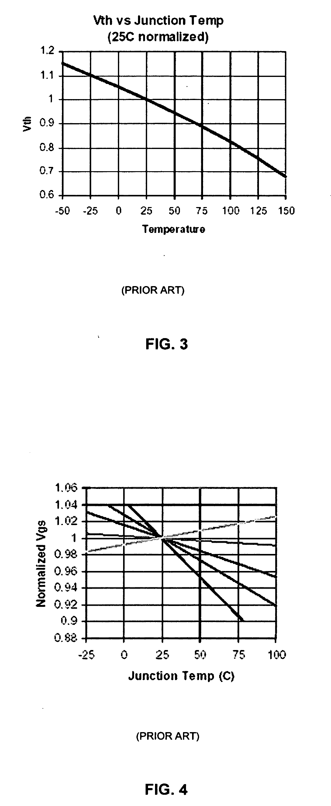
[0081] The description below explains certain features of the invention by providing examples using MOSFET devices, properties and characteristics. It should be understood, however, that the concepts and embodiments of the invention described herein apply to many other types of semiconductor devices, including but limited to controllable semiconductors, three terminal semiconductors, and such power semiconductors as Bipolar Junction Transistors (BJTs), Insulated Gate Bipolar Transistors (IGBTs), Gate Turnoff (GTO) thyristors, and Emitter Turnoff (ETO) thyristors.

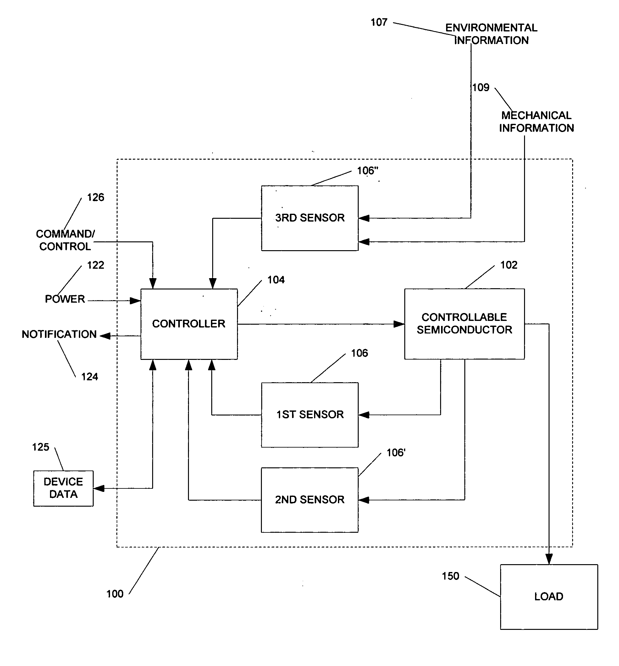
[0082] In one aspect, the invention provides new features that add a level of functionality to conventional power semiconductors and defines and enables a new class of reconfigurable power systems. The new class of reconfigurable power systems includes a device that is referred to hereafter as an Integrated Smart Power Switch (ISPS). At least some implementations of the ISPS can help to resolve various problems of common po...


PUM


Abstract

A device including a controllable semiconductor, sensor, and controller is provided. The controllable semiconductor is associated with a first operating parameter and a second operating parameter, wherein at least the first operating parameter is controllable. The sensor is in communication with the controllable semiconductor device and acquires data relating to the second operating parameter of the controllable semiconductor device. The controller is in communication with the controllable semiconductor device and the sensor, and the controller is configured to access device data associated with the controllable semiconductor, control the first operating parameter of the controllable semiconductor, and receive data from the first sensor relating to the second operating parameter. The controller determines a first predicted value dependent on the device data, compares the data relating to the second operating parameter with the first predicted value, and, if a first condition is detected based on this comparison, dynamically modifies the first operating parameter.

Description

CROSS REFERENCE TO RELATED APPLICATIONS [0001] Not applicable STATEMENT REGARDING FEDERALLY SPONSORED RESEARCH [0002] Not Applicable. FIELD OF THE INVENTION [0003] Embodiments of the invention generally relate to semiconductors and systems. More particularly, the invention relates to systems, methods, and devices for operating, controlling, and monitoring power semiconductors and systems. BACKGROUND OF THE INVENTION [0004] Power semiconductor devices are well known to those of ordinary skill in the art and are commonly used for electronic power conversion, regulation, and control. As building blocks of power systems, power semiconductor devices operate in both a switching mode and a linear mode. Power semiconductors satisfy such conflicting requirements as low weight and volume, high circuit-level reliability, fault isolation, and diagnostic capabilities. [0005] Power transistors are a type of power semiconductor that is used in a variety of applications in the power range from watt...

Claims


Application Information

Patent Timeline
Patent Type & Authority Applications(United States)
IPC IPC(8): H02H3/00
CPCG01K7/42G01R31/046G01R31/2621H01L23/34H03K17/0822H01L2924/0002H03K17/18H03K2017/0806H01L2924/00G01R31/70H03K17/082
Inventor JACOBSON, BORIS S.
Owner RAYTHEON CO
Why Eureka
Try Eureka