Semiconductor devices based on coalesced nano-rod arrays

a technology of nano-rod arrays and semiconductors, applied in nanoinformatics, instruments, optical elements, etc., can solve the problems of low probability of successful wire positioning, complex wire transfer to the substrate, and complex wire growth

Inactive Publication Date: 2006-10-05
RGT UNIV OF CALIFORNIA
View PDF8 Cites 140 Cited by
  • Summary
  • Abstract
  • Description
  • Claims
  • Application Information

AI Technical Summary

Problems solved by technology

Using this approach, wire growth, wire transfer to the substrate and actual device selection are very complicated, and the probability of a successful wire positioning is low.
Consequently, the approach is well suited for demonstration purposes, but is not attractive for device fabrication in an industrial setting.

Method used


Image

  • Semiconductor devices based on coalesced nano-rod arrays
  • Semiconductor devices based on coalesced nano-rod arrays
  • Semiconductor devices based on coalesced nano-rod arrays

Examples


Embodiment Construction

[0022] In the following description of the preferred embodiment, reference is made to the accompanying drawings which form a part hereof, and in which is shown by way of illustration a specific embodiment in which the invention may be practiced. It is to be understood that other embodiments may be utilized and structural changes may be made without departing from the scope of the present invention.

[0023] Overview

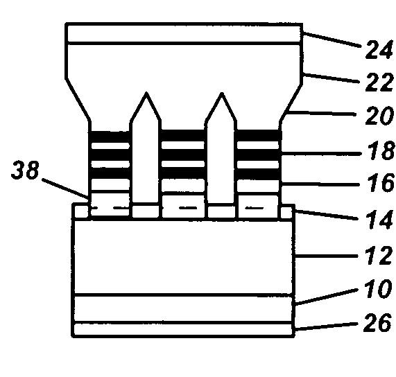
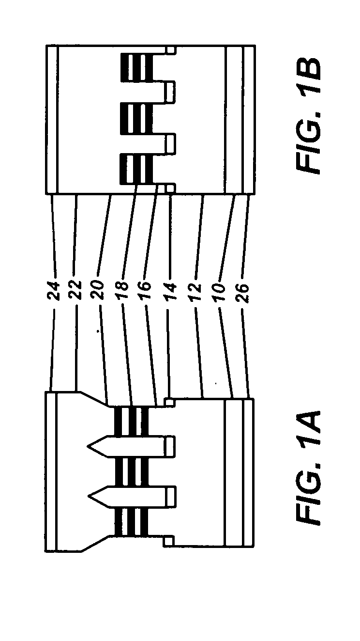
[0024] Semiconductor devices are fabricated using semiconductor nano-rod arrays, wherein the nano-rods are fabricated by growth or etching, and then are coalesced or merged into a continuous planar layer. This approach combines the advantages of nanostructures, which allow the combination of materials with large lattice mismatch while maintaining high crystalline perfection, with the simplicity of device processing for planar epitaxial layers, thereby significantly widening device design opportunities. In addition, this method allows for a significant reduction in contact ...


PUM


Abstract

Semiconductor devices are fabricated using semiconductor nano-rod arrays, which are merged through coalescence into a continuous planar layer after the nano-rods in the nano-rod array are fabricated by growth or etching. Merging of the nano-rods through coalescence into a continuous layer is achieved by tuning the growth conditions into a regime allowing epitaxial lateral overgrowth.

Description

CROSS-REFERENCE TO RELATED APPLICATION [0001] This application claims the benefit under 35 U.S.C. §119(e) of the following co-pending and commonly-assigned application: [0002] U.S. Provisional Application Ser. No. 60 / 632,594, filed on Dec. 2, 2004, by Umesh K. Mishra and Stacia Keller, entitled “SEMICONDUCTOR DEVICES BASED ON COALESCED NANO-ROD ARRAYS,” attorneys' docket number 30794.125-US-P1(2005-218-1); which application is incorporated by reference herein.STATEMENT REGARDING SPONSORED RESEARCH AND DEVELOPMENT [0003] The present invention was made under support from the University of California, Santa Barbara Solid State Lighting and Display Center member companies, including Stanley Electric Co., Ltd., Mitsubishi Chemical Corp., Rohm Co., Ltd., Cree, Inc., Matsushita Electric Works, Matsushita Electric Industrial Co., and Seoul Semiconductor Co., Ltd.BACKGROUND OF THE INVENTION [0004] 1. Field of the Invention [0005] The present invention relates to semiconductor devices based o...

Claims


Application Information

Patent Timeline
IPC IPC(8): H01L21/00
CPCB82Y10/00H01L33/20G02B6/1225H01L21/0237H01L21/02378H01L21/02458H01L21/02505H01L21/0254H01L21/02639H01L21/0265H01L29/0665H01L29/0673H01L29/0676H01L29/068H01L29/2003H01L33/007H01L33/08B82Y20/00
Inventor MISHRA, UMESH KUMARKELLER, STACIA
Owner RGT UNIV OF CALIFORNIA
Why Eureka
Try Eureka